

Solid-state imaging device and method for manufacturing the same
A technology of imaging device and manufacturing method, which is applied in semiconductor/solid-state device manufacturing, radiation control devices, semiconductor/solid-state device components, etc., can solve the problems of lowering, insufficient ability of wiring layer light-shielding film to prevent light incident, and achieve guarantee The effect of shading
- Summary
- Abstract
- Description
- Claims
- Application Information
AI Technical Summary
Problems solved by technology
Method used
Image

Examples
Embodiment Construction
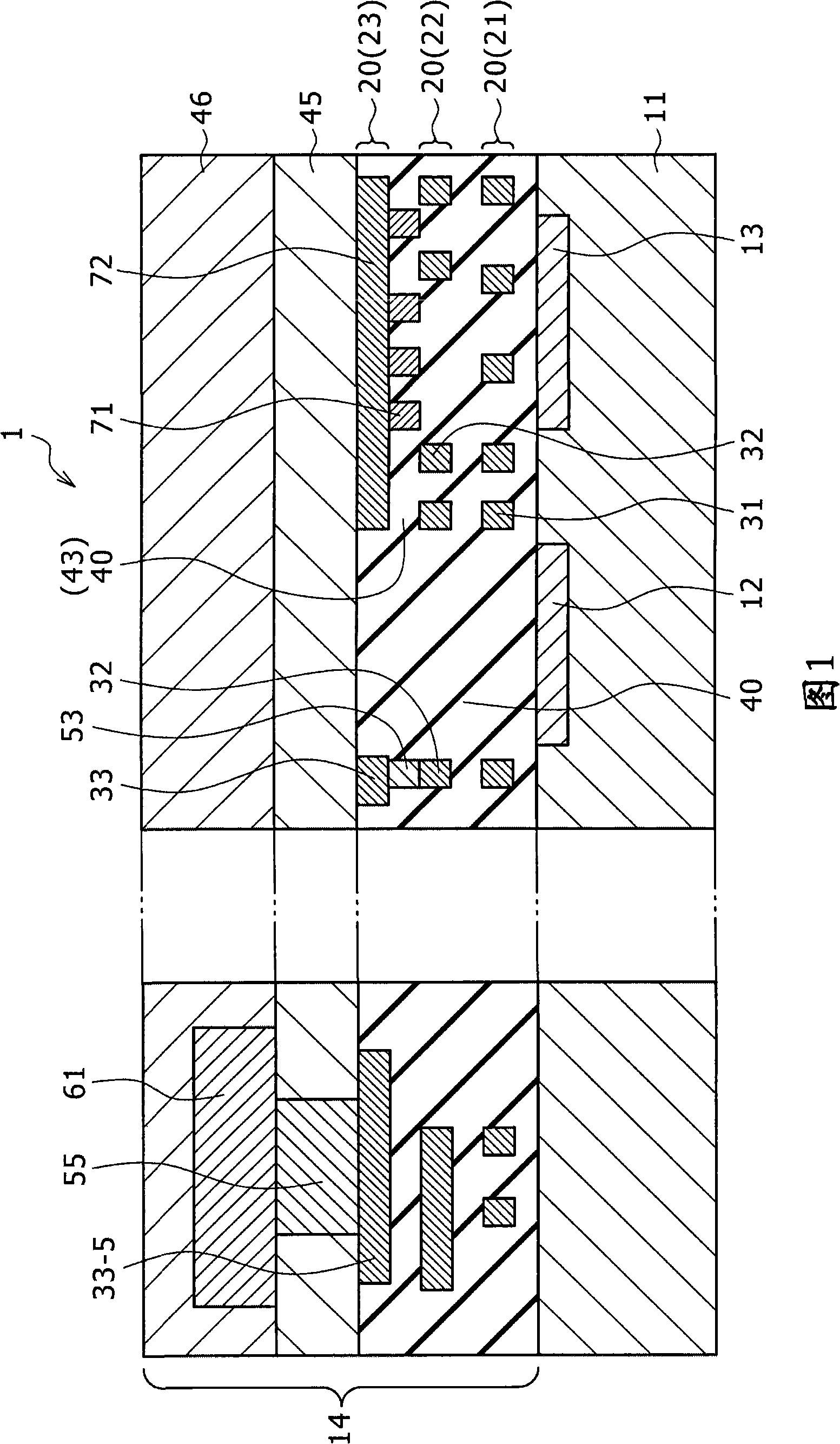
[0054] A first embodiment of the present invention relating to the first solid-state imaging device described above will be described below with reference to FIG. 1 , which is a cross-sectional view of a schematic configuration of the first embodiment. FIG. 1 illustrates a CMOS image sensor as one example of a solid-state imaging device.
[0055] As shown in FIG. 1 , the first solid-state imaging device 1 includes a light receiving pixel section 12 and a black level reference pixel section 13 formed on a semiconductor substrate 11 and composed of photodiodes. Furthermore, the first solid-state imaging device 1 includes a multilayer wiring section 14 formed on the upper surfaces of the light receiving pixel section 12 and the black level reference pixel section 13 .
[0056] The multilayer wiring portion 14 includes a plurality of metal wiring layers 20 (for example, a first metal wiring layer 21 , a second metal wiring layer 22 ( corresponds to the first metal wiring layer in...
PUM
 Abstract
Description
Claims
Application Information