Method for manufacturing LED chips

A technology for light-emitting diodes and manufacturing methods, applied in electrical components, circuits, semiconductor devices, etc., can solve problems such as large differences in refractive index and inability to export chips, and achieve the effects of reducing interface reflection, reducing internal absorption, and improving defects

Active Publication Date: 2009-08-26
EPILIGHT TECH
View PDF0 Cites 14 Cited by
  • Summary
  • Abstract
  • Description
  • Claims
  • Application Information

AI Technical Summary

Problems solved by technology

[0002] Light-emitting diodes have the advantages of small size, high efficiency and long life, and are widely used in traffic indication, outdoor full-color display and other fields. In particular, the use of high-power light-emitting diodes may realize semiconductor solid-state lighting, causing a revolution in the history of human lighting, thus It has gradually become a research hotspot in the field of electronics. In order to obtain high-brightness LEDs, the key is to improve the internal quantum efficiency and external quantum efficiency of the device. At present, the light extraction efficiency of the chip is the main factor limiting the external quantum efficiency of the device. The main reason is The refractive index difference between the epitaxial material, the substrate material and the air is large, resulting in the total reflection of the light generated in the active area at the interface of different refractive index materials and cannot be exported to the chip.

Method used


Image

  • Method for manufacturing LED chips
  • Method for manufacturing LED chips
  • Method for manufacturing LED chips

Examples


Embodiment 1

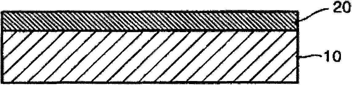
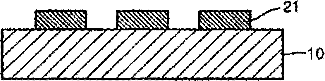
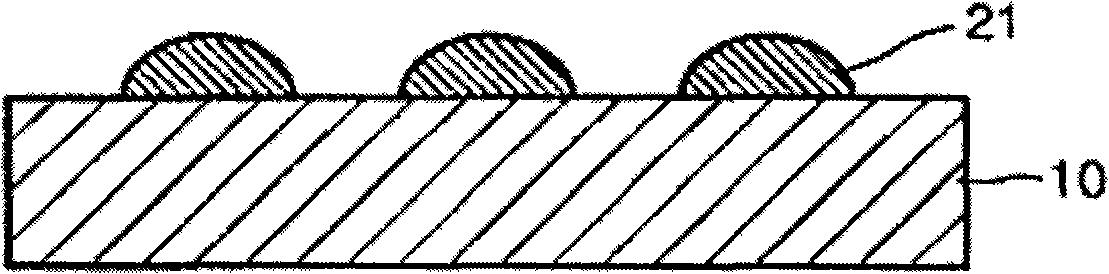
[0029] First refer to Figure 1a As shown, a photoresist is coated on the sapphire substrate 10 to form a layer of photoresist film layer 20. The thickness of the photoresist film layer 20 is 0.5um, and the photoresist is patterned on the substrate by photolithography technology. , forming the desired pattern as Figure 1b As shown, the pattern is a periodic regular arrangement of cylinders. Then use the platform baking photoresist reflow technology to form the photoresist pattern similar to Figure 1c A plurality of convex-hull microstructure patterns 21 are shown. The reflux condition is as follows: the baking temperature is 50° C., and the baking time is 0.1 minute. This pattern was then transferred to sapphire using coupled plasma reactive ion etching as Figure 1d As shown, a plurality of convex hull-shaped microstructures 11 are formed on the surface of the sapphire substrate 10, and the front side of the microstructures 11 is in the shape of a yurt, and its cross-se...

Embodiment 2

[0032] refer to Figure 1a As shown, a photoresist is coated on the sapphire substrate 10 to form a photoresist film layer 20, the thickness of the photoresist film layer 20 is 2um, and the photoresist is patterned on the substrate by photolithography technology , forming the desired pattern as Figure 1b As shown, the pattern is pyramids arranged regularly and periodically. Then use the platform baking photoresist reflow technology to form the photoresist pattern similar to Figure 1c A plurality of convex-hull microstructure patterns 21 are shown. The reflow conditions are as follows: the baking temperature is 200° C., and the baking time is 20 minutes. This pattern was then transferred to sapphire using coupled plasma reactive ion etching as Figure 1d As shown, a plurality of convex hull-shaped microstructures 11 are formed on the surface of the sapphire substrate 10, and the front surface of the microstructures 11 is yurt-shaped, and the cross-section is arc-shaped. ...

Embodiment 3

[0035] refer to Figure 1a As shown, a photoresist is coated on the sapphire substrate 10 to form a photoresist film layer 20, the thickness of the photoresist film layer 20 is 4um, and the photoresist is patterned on the substrate by photolithography technology , forming the desired pattern as Figure 1b As shown, the pattern is periodically and regularly arranged prisms. Then use the platform baking photoresist reflow technology to form the photoresist pattern similar to Figure 1c A plurality of convex-hull microstructure patterns 21 are shown. The reflow conditions are as follows: the baking temperature is 400° C., and the baking time is 60 minutes. This pattern was then transferred to sapphire using coupled plasma reactive ion etching as Figure 1d As shown, a plurality of convex hull-shaped microstructures 11 are formed on the surface of the sapphire substrate 10, and the front surface of the microstructures 11 is yurt-shaped, and the cross-section is arc-shaped. Th...


PUM


Abstract

The invention relates to a method for manufacturing LED chips, comprising the following steps: manufacturing convex-hull periodically arranged microstructures on the surface of a sapphire substrate, and forming a buffer layer on the upper surface of the substrate, an n-type semiconductor layer on the buffer layer, a luminous layer on one part of the n-type semiconductor layer, a p-type semiconductor layer on the luminous layer, and n-type and p-type electrodes on the other part of the n-type semiconductor layer and the p-type semiconductor layer respectively. The yurt-shaped periodically arranged microstructures on the substrate are capable of reducing boundary reflection and internal absorption, effectively improving the defect of epitaxial growth, thus increasing the luminous efficiency of the LED chips.

Description

technical field [0001] The invention relates to a method for manufacturing a light-emitting diode chip, in particular to a method for improving chip luminous efficiency by changing the substrate structure. Background technique [0002] Light-emitting diodes have the advantages of small size, high efficiency and long life, and are widely used in traffic indication, outdoor full-color display and other fields. In particular, the use of high-power light-emitting diodes may realize semiconductor solid-state lighting, causing a revolution in the history of human lighting, thus It has gradually become a research hotspot in the field of electronics. In order to obtain high-brightness LEDs, the key is to improve the internal quantum efficiency and external quantum efficiency of the device. At present, the light extraction efficiency of the chip is the main factor limiting the external quantum efficiency of the device. The main reason is The refractive index difference between the ep...

Claims


Application Information

Patent Timeline
Patent Type & Authority Applications(China)
IPC IPC(8): H01L33/00
Inventor 袁根如郝茂盛颜建锋李士涛陈诚董云飞
Owner EPILIGHT TECH
Why Eureka
Try Eureka