Method for manufacturing multilayer electronic component
A technology of electronic components and manufacturing methods, which is applied to the manufacture of capacitors, fixed capacitance parts, electrical components, etc., can solve the problems of high equipment costs, complicated procedures, waste of materials, etc., and achieve the effect of easy automation of pressurization
- Summary
- Abstract
- Description
- Claims
- Application Information
AI Technical Summary
Problems solved by technology
Method used
Image
Examples
no. 1 Embodiment approach
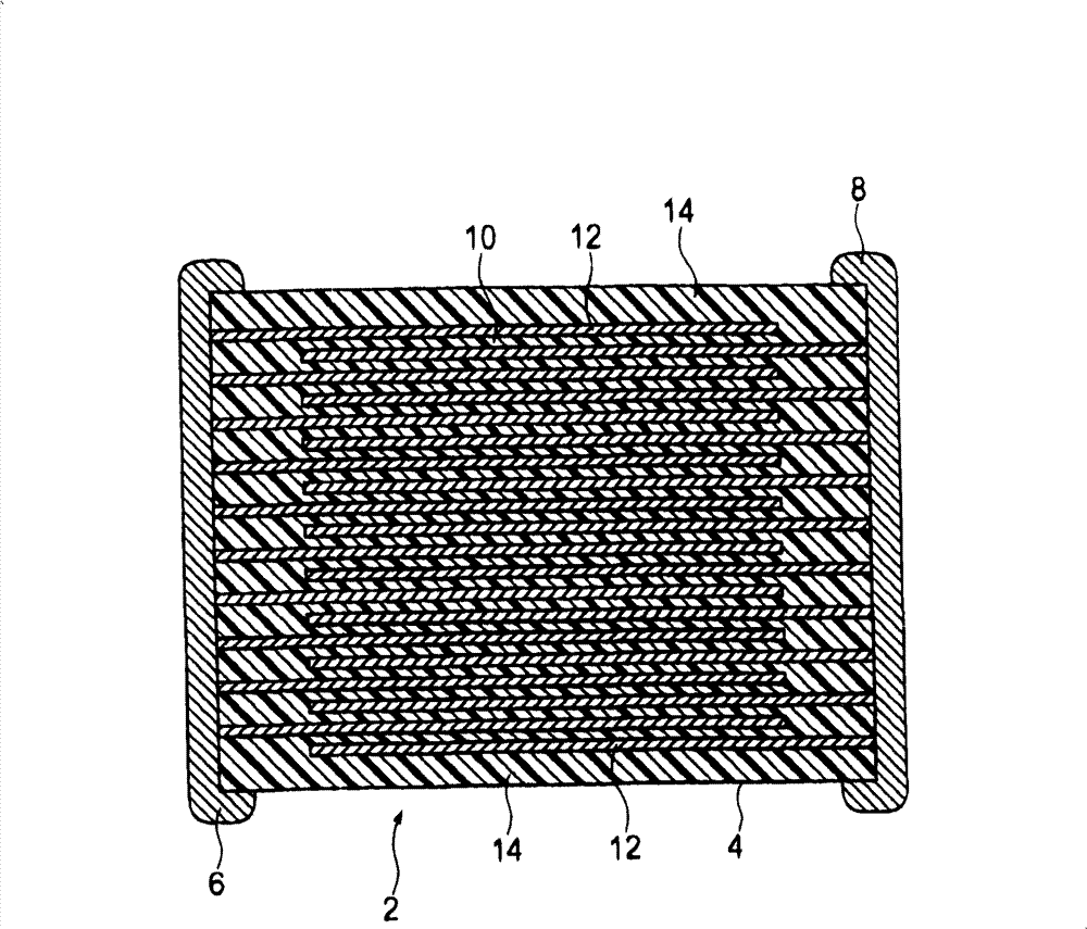
[0022] First, an overall configuration of a laminated ceramic capacitor will be described as one of the embodiments of the laminated electronic component manufactured by the method according to the embodiment of the present invention.
[0023] Such as figure 1 As shown, the laminated ceramic capacitor 2 of the present embodiment has a capacitor body (element body) 4 , a first terminal electrode 6 , and a second terminal electrode 8 . The capacitor blank 4 has internal electrode layers 12 which are alternately laminated between inner dielectric layers 10 .
[0024] The capacitor body 4 has outer dielectric layers 14 on both end faces in the lamination direction. One of the internal electrode layers 12 laminated in a zigzag pattern is electrically connected to the inner side of the first terminal electrode 6 formed on the outer side of the first end portion of the capacitor body 4 . Furthermore, the other internal electrode layer 12 laminated in a staggered manner is electrica...
no. 2 Embodiment approach
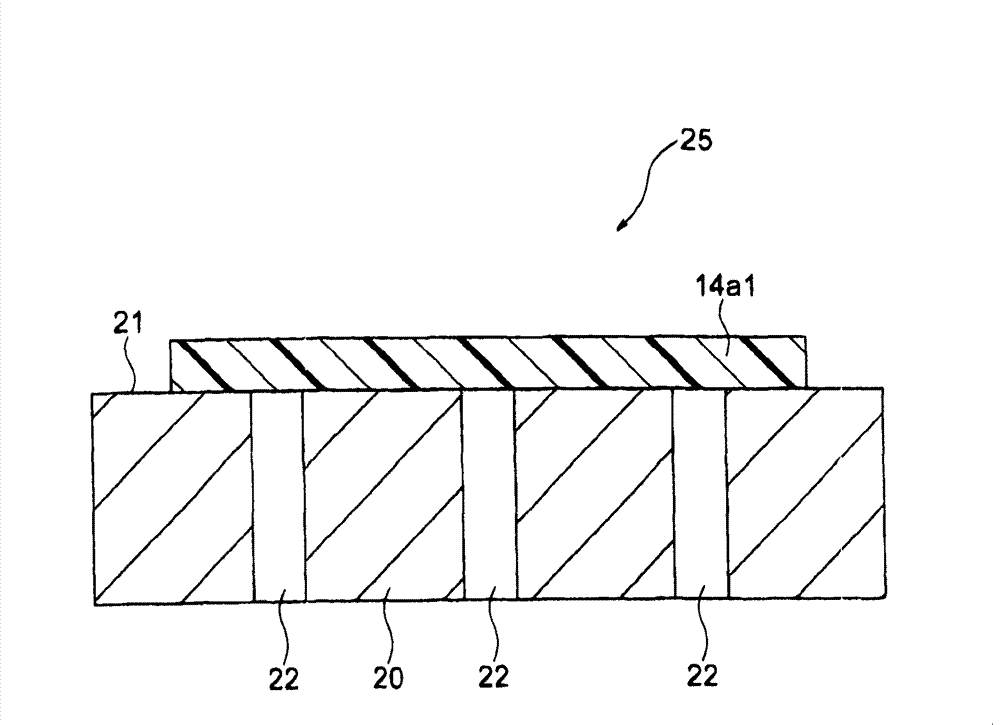
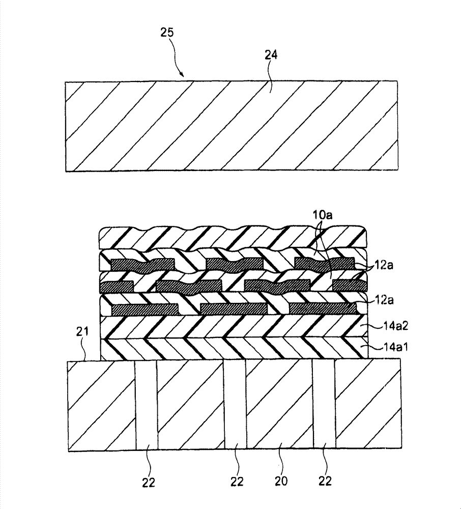
[0051] In the second embodiment of the present invention, after laminating figure 2 Before the die 25 shown, only the outer green sheet 14a1 to be laminated on the lowermost side is dried in advance under different conditions from the other green sheets 14a2, 10a, 14a3, and 14a4. That is, the outer green sheet 14a1 is dried under drying conditions in which the adhesive force of the outer green sheet 14a1 becomes weaker than that of the other green sheets 14a2, 10a, 14a3, and 14a4. By changing the drying conditions in this way, the outer green sheet 14a1 can also be made weaker in adhesive force than the other green sheets 14a2, 10a, 14a3, and 14a4.
[0052] Specifically, only the outer green sheet 14a1 is previously dried at a higher drying temperature and / or for a longer drying time than the other green sheets 14a2, 10a, 14a3, and 14a4. More specifically, the dielectric slurry was dried at about 90° C. for 5 seconds to form a green sheet. Other configurations and effects a...
no. 3 Embodiment approach
[0054] In the third embodiment of the present invention, the thickness of the outer green sheet 14a1 to be laminated on the lowermost side is made thinner than the thickness of the other outer green sheets 14a2. Specifically, the thickness of the outer green sheet 14a1 is reduced to about 20% to 80% of the thickness of the other outer green sheet 14a2. More specifically, when the thickness of the outer green sheet 14a2 is 5 μm to 15 μm, the thickness of the outer green sheet 14a1 is 1 μm to 12 μm. In order to form a thin sheet, it is possible to change the discharge amount of the doctor blade or to increase the travel speed of the film during dielectric slurry coating.
[0055] By varying the thickness of the same outer green sheets in this way, the outer green sheet 14a1 has a weaker adhesive force than the other green sheets 14a2, 10a, 14a3, and 14a4. Other configurations and effects are the same as those of the first embodiment. In addition, since the thickness of the she...
PUM
| Property | Measurement | Unit |
|---|---|---|
| glass transition temperature | aaaaa | aaaaa |
Abstract
Description
Claims
Application Information
 - R&D
- Intellectual Property
- Life Sciences
- Materials
- Tech Scout
- Unparalleled Data Quality
- Higher Quality Content
- 60% Fewer Hallucinations
Browse by: Latest US Patents, China's latest patents, Technical Efficacy Thesaurus, Application Domain, Technology Topic, Popular Technical Reports.
© 2025 PatSnap. All rights reserved.Legal|Privacy policy|Modern Slavery Act Transparency Statement|Sitemap|About US| Contact US: help@patsnap.com


