Imaging detector
A technology for imaging detectors and detectors, which is applied in instruments, measuring devices, image communication, etc., can solve the problems of difficulty in manufacturing and obtain commercial devices, and achieve the effects of good absorption and increased sensing efficiency.
- Summary
- Abstract
- Description
- Claims
- Application Information
AI Technical Summary
Problems solved by technology
Method used
Image
Examples
Embodiment Construction
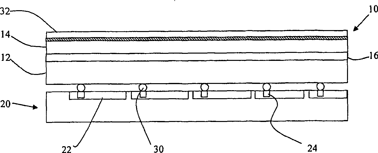
[0031] refer to figure 1 , the sensor 10 is mounted on the readout chip 20 by using a plurality of bump contacts 30, each bump contact corresponding to a single pixel. The readout chip comprises an independent photon counting detector 22 for each pixel and thus each bump contact 30 .
[0032] The sensor 10 comprises two sensor material layers 12 , 14 . The first of these sensor material layers is a silicon substrate 12 and the second sensor material layer is a germanium epitaxial layer 14 . In an embodiment, the substrate 12 is 300 μm thick and the epitaxial layer is 50 μm thick. A thin buffer layer 16 is provided between the substrate 12 and the epitaxial layer 14, the buffer layer has a composition gradient of silicon and germanium, a high silicon content near the silicon substrate 12, and a high Si content near the germanium epitaxial layer 14. Germanium content to minimize lattice strain and deformation.
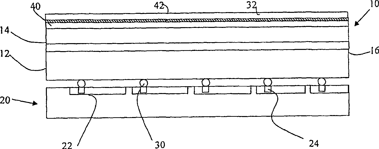
[0033] The ohmic contact 42 is formed by being inserted into th...
PUM
 Abstract
Description
Claims
Application Information


