Electron radiation monitoring system to prevent gold spitting and resist cross-linking during evaporation

US20110193576A1Active Publication Date: 2011-08-11SKYWORKS SOLUTIONS INC

Image

  • Electron radiation monitoring system to prevent gold spitting and resist cross-linking during evaporation
  • Electron radiation monitoring system to prevent gold spitting and resist cross-linking during evaporation
  • Electron radiation monitoring system to prevent gold spitting and resist cross-linking during evaporation

Examples


example

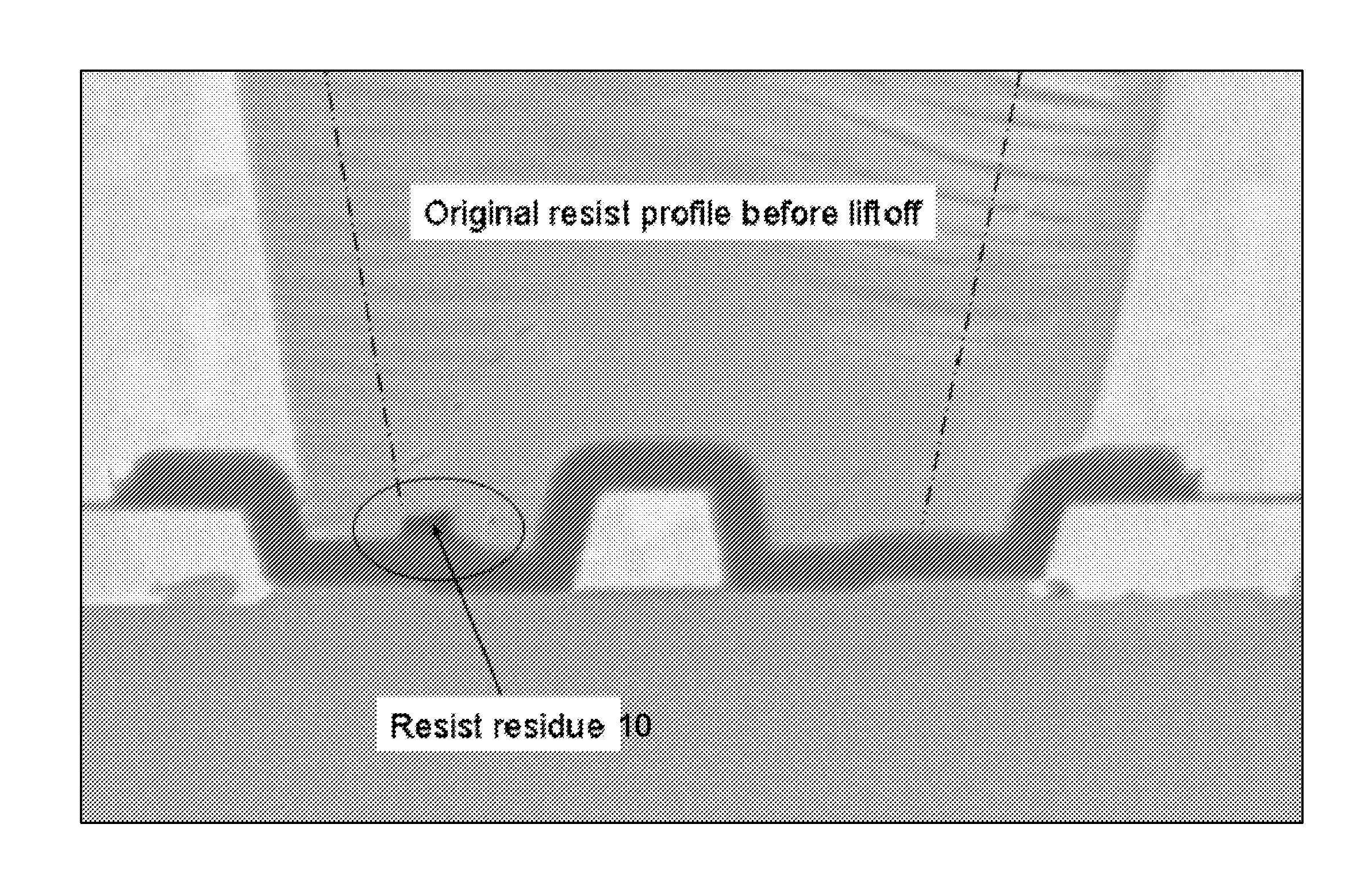
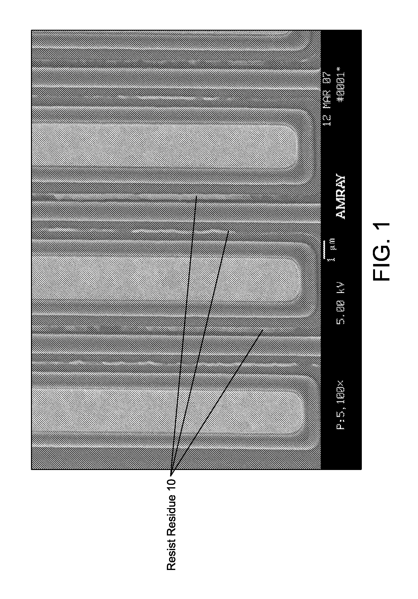
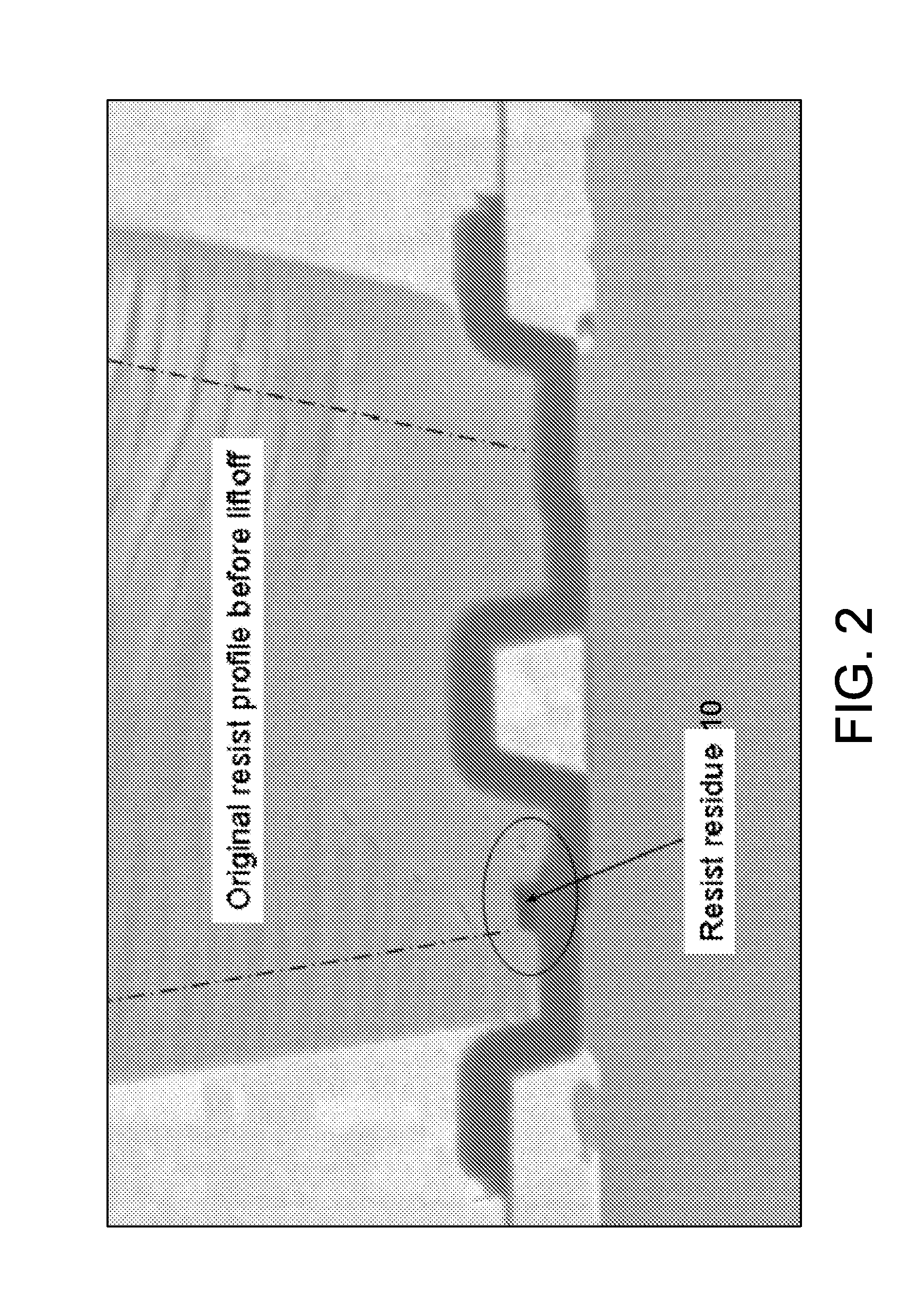
[0109]To investigate the source of backscattered electron radiation, a series of experiments were conducted to compare the amount of energetic free electrons generated from different materials during the evaporation process in an e-beam metal evaporation / deposition system. An electrode was fabricated to fit inside the vacuum chamber of an e-beam metal evaporation / deposition system vacuum. This electrode provided for the comparison of the number of energetic electrons generated from an electron-beam hitting different materials. The electrode was formed from a copper plate bent into a ring. The copper electrode plate was electrically isolated from ground by ceramic standoffs in the vacuum chamber. A copper wire was utilized to connect the electrode to a high-impedance voltmeter with data-logging capability (a Keithley 2420 source meter), where voltage signals from the electrode were monitored and logged in a data file. Since the set up was not calibrated against any certified standard...


PUM

PropertyMeasurementUnit
Concentrationaaaaaaaaaa
Electric potential / voltageaaaaaaaaaa
Threshold limitaaaaaaaaaa

Abstract

Disclosed herein are systems and methods for in-situ measurement of impurities on metal slugs utilized in electron-beam metal evaporation / deposition systems, and for increasing the production yield of a semiconductor manufacturing processes utilizing electron-beam metal evaporation / deposition systems. A voltage and / or a current level on an electrode disposed in a deposition chamber of an electron-beam metal evaporation / deposition system is monitored and used to measure contamination of the metal slug. Should the voltage or current reach a certain level, to the deposition is completed and the system is inspected for contamination.

Description

RELATED APPLICATIONS[0001]This application claims priority under 35 U.S.C. ยง119(e) to U.S. Provisional Application Ser. No. 61 / 303,040, entitled โ€œELECTRON RADIATION MONITORING SYSTEM TO PREVENT GOLD SPITTING AND RESIST CROSS LINKING DURING EVAPORATION,โ€ filed on Feb. 10, 2010, which is herein incorporated by reference in its entirety.BACKGROUND[0002]1. Field of Invention[0003]The present disclosure relates generally to metal deposition systems and, more specifically, to systems and methods for the detection and / or rectification of conditions caused by impurities in metal evaporation sources used in electron-beam metal evaporation / deposition.[0004]2. Discussion of Related Art[0005]Various steps in the processing of semiconductor wafers to form microchips for use in electronic devices involve the deposition of one or more layers of metal on the semiconductor wafers. These metal films are used to form, for example, metal contacts or conductive pathways. Metal films are deposited on sem...

Claims


Application Information

Patent Timeline
11 Aug 2011
Publication
US20110193576A1
IPC
G01R27/08
CPC
H01J37/304; H01J37/3053; H01J2237/30472; Y10T29/41; G01N27/00; H01L21/02; H01J2237/3132; H01J2237/24475
Inventors
CHENG, KEZIA