Metal electronic tag antenna
An electronic tag and anti-metal technology, which is applied in the field of microwave communication, can solve the problems of large size, inconvenient use, and large thickness of anti-metal electronic tag antennas, and achieve the effects of small size, wide application range, and increased radiation area
- Summary
- Abstract
- Description
- Claims
- Application Information
AI Technical Summary
Problems solved by technology
Method used
Image
Examples
Embodiment Construction
[0016] The present invention will be further described in detail below in conjunction with the drawings and specific embodiments.
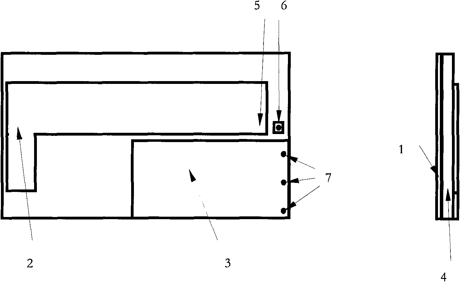
[0017] figure 1 It is a schematic diagram of the structure of an anti-metal electronic tag antenna. As shown in the figure, the antenna is divided into three layers: the bottom layer, the top layer, and the middle layer. The bottom layer is a complete metal conductor, such as copper foil, which forms the floor 1 of the microstrip antenna. The top layer is composed of three independent metal conductors such as copper foil, including two arms of the dipole antenna and a square pad 6. The first arm 2 of the dipole antenna and the main radiator 2 of the microstrip antenna are the same A piece of metal conductor, which is also the main radiator of the anti-metal electronic tag antenna of the present invention, and the second arm 3 of the dipole antenna is DC short-circuited between the floor 1 through a via hole. The square pad 6 and the floor 1 are DC s...
PUM
 Abstract
Description
Claims
Application Information

