Anomaly detection method of UV photoresist hardening platform

A photoresist and anomaly technology, which is applied in the field of abnormal detection of UV photoresist hardening machines, can solve problems such as photoresist flow, and achieve the effect of improving the yield of hardened products

Active Publication Date: 2009-09-16
HEJIAN TECH SUZHOU
View PDF0 Cites 0 Cited by
  • Summary
  • Abstract
  • Description
  • Claims
  • Application Information

AI Technical Summary

Problems solved by technology

[0004] In view of the existing defects of the above-mentioned prior art, the purpose of the present invention is to provide a method for detecting abnormality of a UV photoresist hardening machine, so as to solve the

Method used


Image

  • Anomaly detection method of UV photoresist hardening platform
  • Anomaly detection method of UV photoresist hardening platform
  • Anomaly detection method of UV photoresist hardening platform

Examples


Embodiment Construction

[0020] In order to make the above-mentioned purposes, features and advantages of the present invention more obvious and easy to understand, below in conjunction with a preferred embodiment of the present invention, the detailed description is as follows:

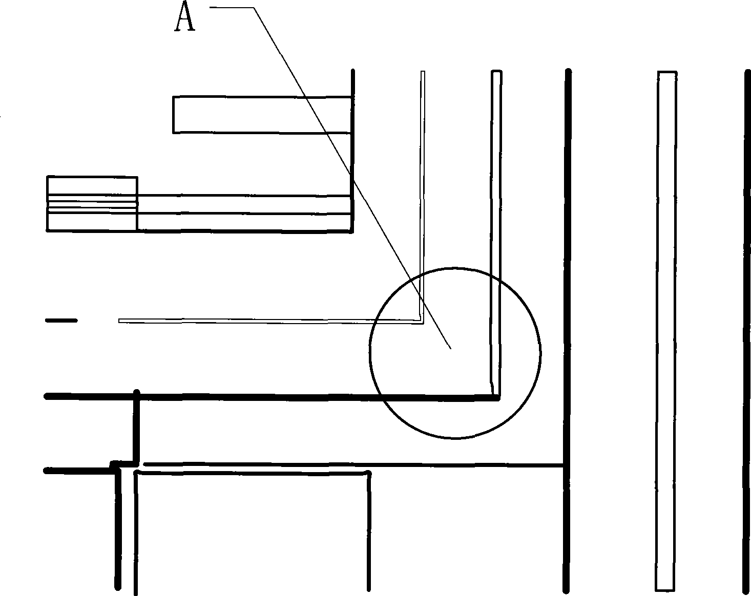
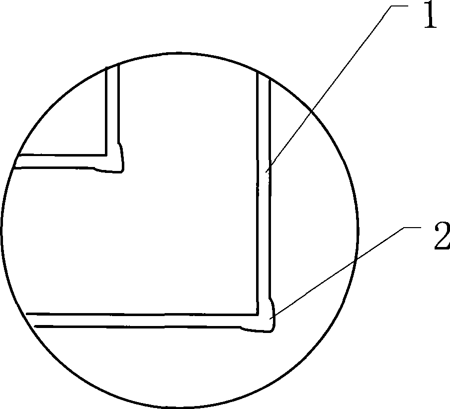
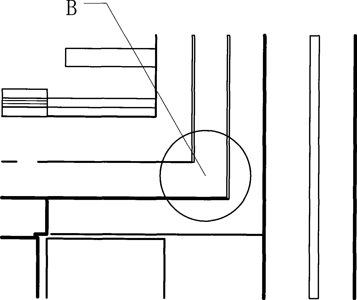
[0021] In the pre-sequence process of semiconductor manufacturing, photoresist is evenly coated on the wafer with a very thin thickness to make the silicon wafer photosensitive, and then the lens and the photolithographic mask with the designed circuit are used to process the photoresist under UV light. Under the irradiation, the circuit pattern is copied to the surface of the silicon wafer and developed. Before subsequent etching or ion implantation, the photoresist film needs to be hardened by a UV photoresist hardening machine. However, during the processing of the UV photoresist hardening machine, there are sometimes abnormal situations. Due to the influence of abnormalities such as too weak UV light or too high temperat...


PUM


Abstract

The invention discloses an anomaly detection method of a UV photoresist hardening platform; the method comprises the following steps: a predetected photoresist film is used as detecting medium, and a difference value of amount of shrinkage and the degree of change of optical characteristics of the predetected photoresist film before and after UV hardening treatment is measured and compared, thus realizing the control to the working condition of the UV photoresist hardening platform, wherein the predetected photoresist film is a photoresist coating layer on a non-IC image wafer disk; the difference value of the amount of shrinkage is embodied on the change of the thickness of the predetected photoresist; the change of the optical characteristics is embodied on the degree of change of refractive index and reflection index and the like. The design proposal can pre-judge and control the influence degree of anomaly of the UV hardening platform from detecting results, improve the hardening yield of the photosensitive silicon wafer photoresist by statistics of the different value and control of manufacture procedures, reduce photoresist flow to the utmost and reduce the probability of forming convex sharp angles.

Description

technical field [0001] The invention relates to semiconductor manufacturing, in particular to a method for detecting abnormality of a UV photoresist hardening machine. Background technique [0002] In the semiconductor manufacturing process, especially in the pre-order wafer process, the silicon wafer that has been drawn, sliced, ground, and oxidized by a single crystal silicon rod needs to be evenly coated with a photosensitive adhesive (hereinafter referred to as photoresist) in an extremely thin thickness. Distributed on it to make the silicon wafer photosensitive, the subsequent circuit layout photolithography process can be carried out. Under the irradiation of UV light, the lens and the photolithographic mask with designed circuit form a very small and dense circuit pattern on the surface of the photosensitive silicon wafer. In this way, the photosensitive silicon wafer that has undergone photoetching can continue to undergo a series of process steps such as subsequen...

Claims


Application Information

Patent Timeline
IPC IPC(8): G03F7/40G03F7/26G01B21/08G01M11/02
Inventor 陈伏宏
Owner HEJIAN TECH SUZHOU
Why Eureka
Try Eureka