Structure of semiconductor chip with silicon through hole and stacking assembly thereof

A semiconductor and through-silicon via technology, used in semiconductor devices, semiconductor/solid-state device components, electrical solid-state devices, etc., can solve problems such as poor process yield and difficult chip alignment, avoid displacement, and reduce stacking height. , The effect of easy stacking alignment

Inactive Publication Date: 2009-09-16
POWERTECH TECHNOLOGY
View PDF2 Cites 21 Cited by
  • Summary
  • Abstract
  • Description
  • Claims
  • Application Information

AI Technical Summary

Problems solved by technology

Once one of the semiconductor chip structures 100 is stacked and one of the conductive pins 12 is distorted, the through holes 113 of the subsequent stacked semiconductor chip structures 100 cannot be smoothly penetrated by these conductive pins 12, so there are difficulties in chip alignment and poor process. poor rate problem

Method used


Image

  • Structure of semiconductor chip with silicon through hole and stacking assembly thereof
  • Structure of semiconductor chip with silicon through hole and stacking assembly thereof
  • Structure of semiconductor chip with silicon through hole and stacking assembly thereof

Examples


no. 1 Embodiment

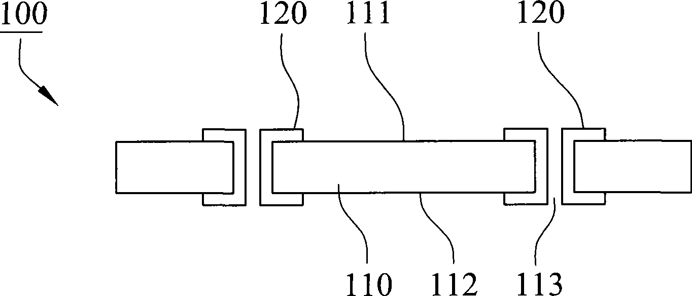
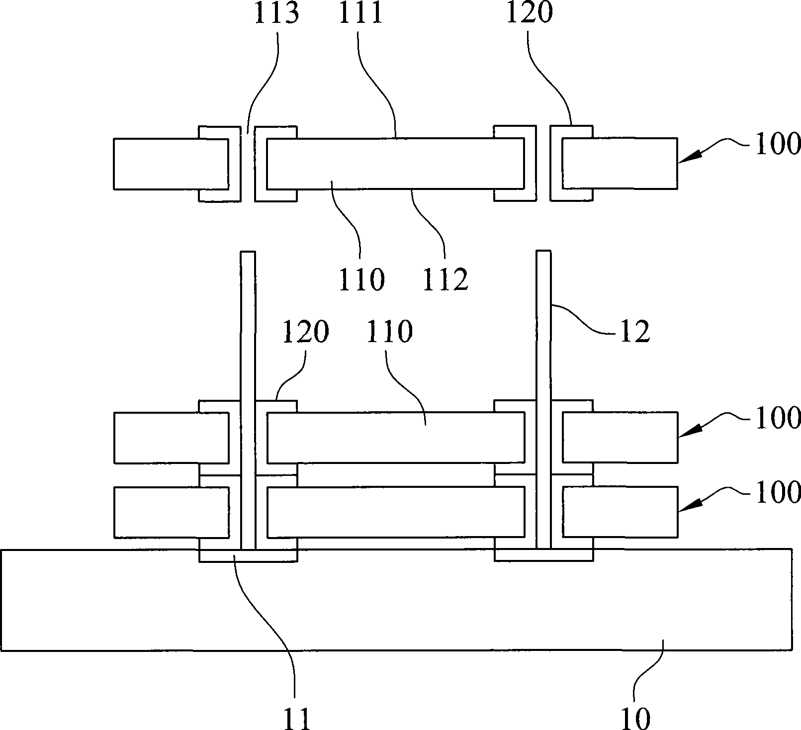
[0068] According to a first specific embodiment of the present invention, a semiconductor chip structure with TSVs and a stacking combination thereof are provided. see image 3 As shown, a semiconductor chip structure 200 with through-silicon vias mainly includes a semiconductor substrate 210, two or more first pads 220, two or more second pads 230, two or more The first flange ring 240 and two or more second flange rings 250 . The semiconductor substrate 210 has a first surface 211 , an opposite second surface 212 and two or more through holes 213 passing through the first surface 211 and the second surface 212 . The semiconductor substrate 210 is made of semiconductor material, such as silicon, gallium arsenide and the like. A surface of the semiconductor substrate 210 can be formed with various integrated circuits and can be electrically connected to the first bonding pads 220 and two or more than two second bonding pads 230 . Preferably, the integrated circuit is formed...

no. 2 Embodiment

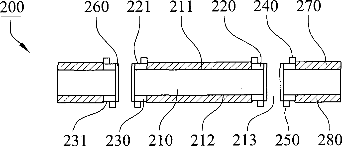
[0077] In the second embodiment of the present invention, another semiconductor chip structure with TSVs and its stacking combination are disclosed. see Figure 8As shown, a semiconductor chip structure 300 with TSVs mainly includes a semiconductor substrate 310 , a first bonding pad 320 , a second bonding pad 330 , a first flange ring 340 and a second flange ring 350 . The semiconductor substrate 310 has a first surface 311 , an opposite second surface 312 , a first half-through hole 313 formed in the first surface 311 , and a second half-through hole 314 formed in the second surface 312 . Specifically, the first half-through hole 313 and the second half-through hole 314 can be half-etched and plated to form blind holes.

[0078] The first pad 320 is disposed on the first surface 311 , and the first half-through hole 313 also penetrates through and vertically corresponds to the first pad 320 . The second welding pad 330 is disposed on the second surface 312 , and the second...


PUM


Abstract

The invention provides a structure of a semiconductor chip with silicon through holes and stacking assembly thereof; two or more through holes vertically penetrate bonding pads on the upper surface and the lower surface of a semiconductor substrate; two or more first flange rings are convexly arranged on the bonding pad which is arranged on the upper surface of the semiconductor substrate, thus leading the corresponding bonding pad to be provided with a contact surface which is arranged between the first flange rings and the through holes; two or more second flange rings are convexly arranged on the bonding pad which is arranged on the lower surface of the semiconductor substrate, thus leading the corresponding bonding pad to be provided with a contact surface which surrounds the outside of the second flange rings; and the second flange rings can be embedded in the first flange rings due to the dimension thereof. By utilizing the embedment of the flange rings, the invention can realize the accurate matchup of the chips and avoid displacement, and also can realize a chip stacking technique of stacking the chips first and then filling the through holes with materials for filling holes, wherein the materials for filling holes does not flow out and no electrical short circuit of the adjacent through holes exists, thus meeting the requirements of micro-interval between silicon through holes.

Description

technical field [0001] The present invention relates to a semiconductor device, in particular to a structure of a semiconductor chip with a through-silicon via (TSV, Through Silicon Via) and a stacking combination thereof. Background technique [0002] In the field of semiconductor electronics, an integrated circuit forms the active surface of a semiconductor chip, and conventional chip terminals, such as bonding pads, are also formed on the active surface. In the high-density electrical interconnection technology of chips, it is desirable to have terminals on both the active surface and the back of the chip for three-dimensional stacking or / and high-density packaging. Therefore, it is proposed that a chip stacking combination structure technology can be developed towards high-precision processes such as high power, high density and miniaturization, that is, through silicon via (TSV, Through Silicon Via) technology. Through-silicon via technology is to open through-holes in...

Claims


Application Information

Patent Timeline
Patent Type & Authority Applications(China)
IPC IPC(8): H01L23/482H01L23/544H01L25/00H01L23/48
CPCH01L2224/13H01L23/481
Inventor 陈酩尧
Owner POWERTECH TECHNOLOGY
Why Eureka
Try Eureka