Large-array CMOS image sensor and manufacturing method thereof

A technology of image sensor and manufacturing method, applied in semiconductor/solid-state device manufacturing, electric solid-state device, semiconductor device and other directions, can solve the problems of circuit damage, large amount of wafer usage, low reliability, etc., to simplify and improve the manufacturing process. Yield and reliability improvement

Inactive Publication Date: 2009-09-16
BRIGATES MICROELECTRONICS KUNSHAN
View PDF0 Cites 4 Cited by
  • Summary
  • Abstract
  • Description
  • Claims
  • Application Information

AI Technical Summary

Problems solved by technology

[0005] 1) In the prior art, the geometric size of the circuit must fully conform to the size of the pixel array, otherwise it cannot be spliced
[0006] 2) Since the pixel array and peripheral circuits must be connected one by one, the wafer usage is large, so the cost is high
[0007] 3) Since the analog circuit and digital circuit graphics are not repeatable, the splicing process is complex, and in the process, the number of masks required will be large, so the cost is high
[0008] 4) In X-ray imaging, rays will cause damage to the circuit, making the circuit work abnormally and reducing reliability
[0009] In summary, the manufacturing process of the above-mentioned CMOS image sensor is difficult, high in cost and low in reliability.

Method used


Image

  • Large-array CMOS image sensor and manufacturing method thereof
  • Large-array CMOS image sensor and manufacturing method thereof
  • Large-array CMOS image sensor and manufacturing method thereof

Examples


Embodiment Construction

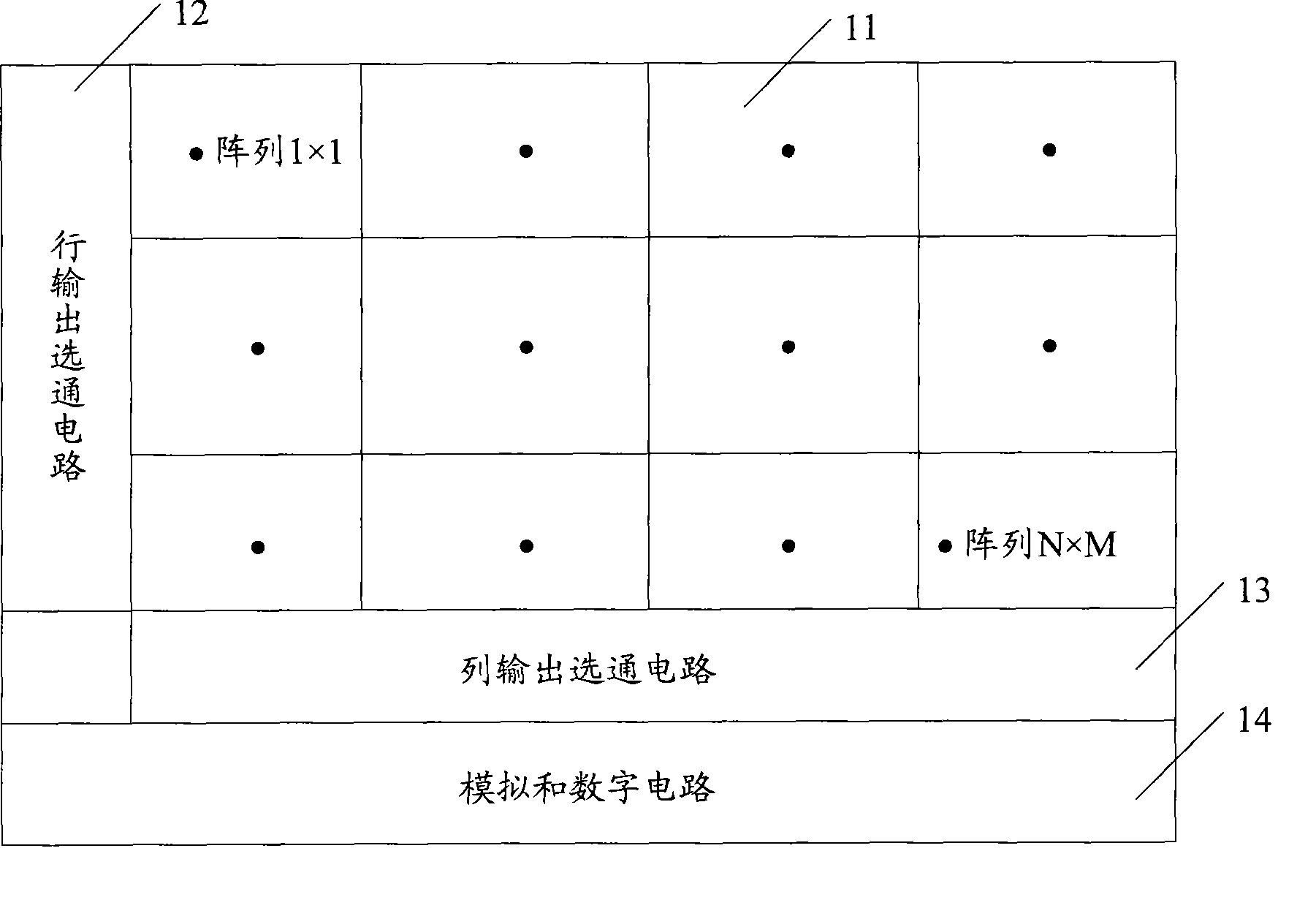
[0032] The present invention provides a large-array CMOS image sensor and its manufacturing method. The core idea of ​​the present invention is to separate the splicing of the pixel array from the peripheral circuit, and complete the function of the peripheral circuit through a single chip, so as to reduce the difficulty of the process and reduce the cost. , to improve the output image quality.

[0033] In order to make the purpose, technical solution and advantages of the present invention clearer and clearer, specific embodiments will be described in detail below with reference to the accompanying drawings.

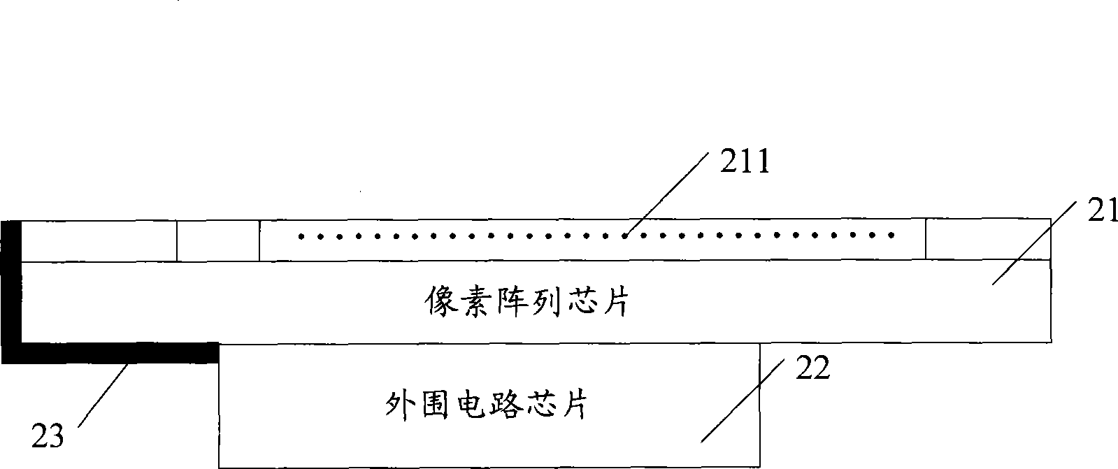
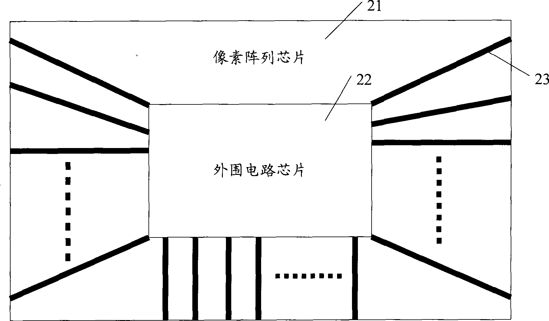
[0034] figure 2 It is a schematic side view of the large array CMOS image sensor in Embodiment 1 of the present invention, image 3 It is the rear view of the large array CMOS image sensor in Embodiment 1 of the present invention, combined below figure 2 and image 3 To illustrate: the CMOS image sensor includes a pixel array chip 21 and a peripheral circuit chip 2...


PUM


Abstract

The invention provides a large-array CMOS image sensor, which comprises a pixel array chip and a peripheral-circuit processing chip, wherein the peripheral-circuit processing chip is positioned on the back of the pixel array chip and is connected with the pixel array chip. The invention also provides a method for manufacturing the large-array CMOS image sensor, which is characterized in that the method comprises the steps of preparing a pixel array into the pixel array chip, preparing a peripheral circuit outside the pixel array into the peripheral-circuit processing chip, placing the peripheral-circuit processing chip on the back of the pixel array chip and connecting the peripheral-circuit processing chip with the pixel array chip. The large-array CMOS image sensor and the manufacturing method thereof have the advantages of simplifying the process difficulty of the CMOS image sensor, reducing cost and improving the reliability of the image sensor.

Description

technical field [0001] The invention relates to the technical field of complementary metal oxide semiconductor (CMOS) image sensors, in particular to a large array CMOS image sensor and a manufacturing method thereof. Background technique [0002] The CMOS image sensor is composed of several units such as pixel array, row and column gating, analog signal amplification and output, and digital signal processing, and is integrated on a chip. Due to the limitation of photolithography process, large array and large size are not easy to realize, so the application is limited, making it difficult to play the advantages of CMOS image sensor. For example, X-ray chest X-ray has begun to develop from film to digital, but since the imaging area needs to adapt to the geometric size of the human body, the area of ​​the image sensor must be large enough. The existing method is to use the technology of thin film field effect transistor (TFT, ThinFilm Transistor) in liquid crystal display (...

Claims


Application Information

Patent Timeline
Patent Type & Authority Applications(China)
IPC IPC(8): H01L25/18H01L23/488H01L27/146H01L21/60
CPCH01L2924/0002
Inventor 周谨
Owner BRIGATES MICROELECTRONICS KUNSHAN
Why Eureka
Try Eureka