Growth method for controlling nucleation of self-organization In-Ga-As quantum dots

A growth method and an indium gallium arsenide technology are applied in the growth field of controlling the nucleation of self-organized indium gallium arsenide quantum dots, which can solve the problems of uneven quantum dot layers, lack of a step of depositing a stress relief layer, etc. range, the effect of improving uniformity

Inactive Publication Date: 2009-09-23
INST OF SEMICONDUCTORS - CHINESE ACAD OF SCI
View PDF0 Cites 8 Cited by
  • Summary
  • Abstract
  • Description
  • Claims
  • Application Information

AI Technical Summary

Problems solved by technology

The growth steps of the prior art Structure B samples were similar to figure 1 The step of (a) just lacks the step of depos...

Method used


Image

  • Growth method for controlling nucleation of self-organization In-Ga-As quantum dots
  • Growth method for controlling nucleation of self-organization In-Ga-As quantum dots
  • Growth method for controlling nucleation of self-organization In-Ga-As quantum dots

Examples


Embodiment Construction

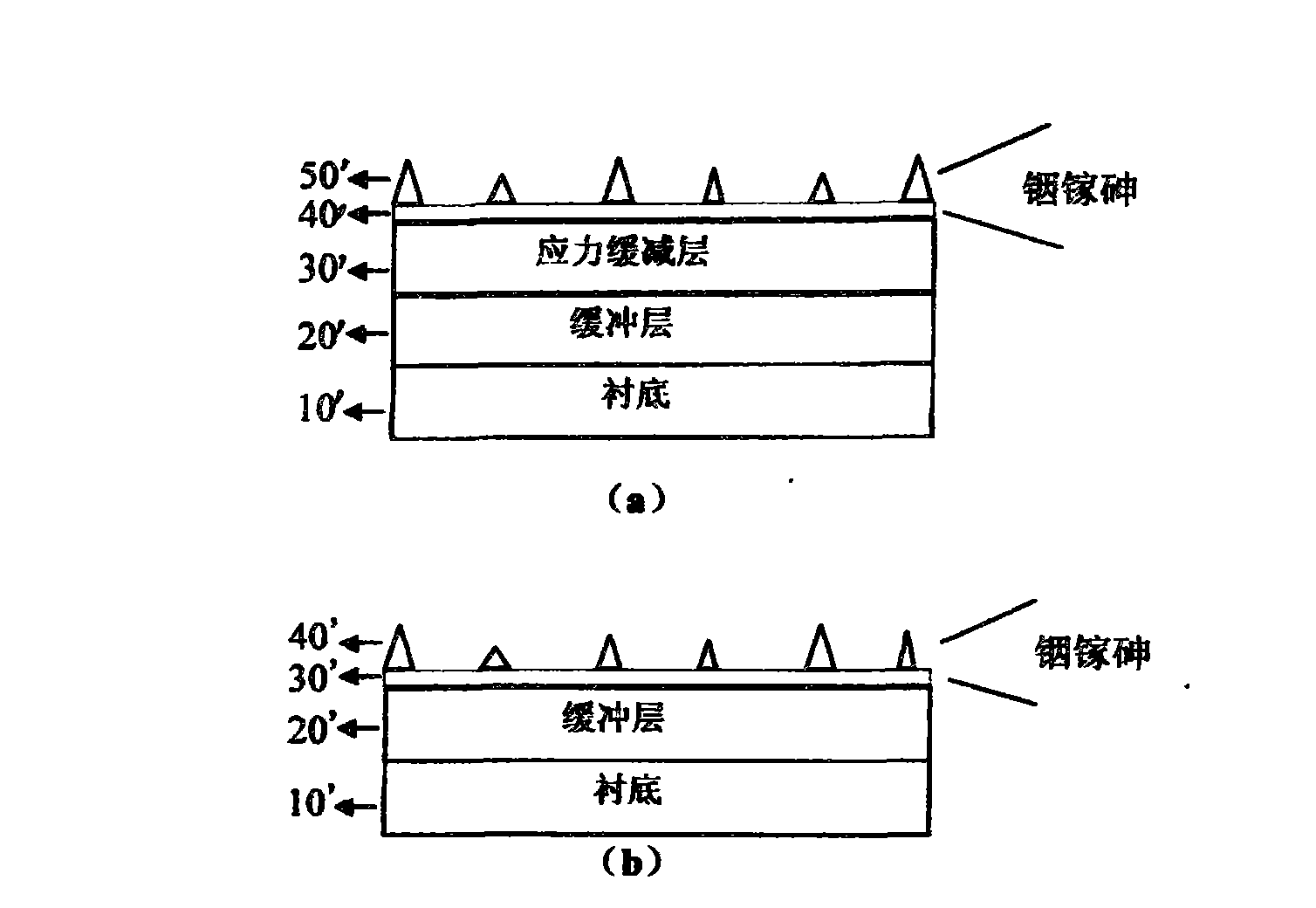
[0036] see figure 2 Shown is the first embodiment of the present invention.

[0037] A growth method for controlling the nucleation of self-organized indium gallium arsenic quantum dots of the present invention comprises the following steps:

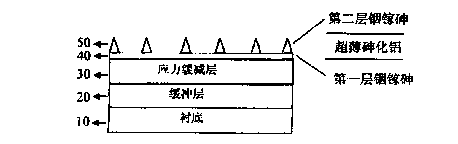
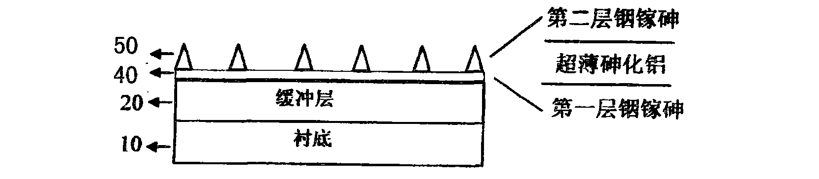
[0038] Step 1: Select a substrate 10, the substrate 10 is a gallium arsenide (001) substrate;

[0039]Step 2: grow a buffer layer 20 on the substrate 10 by molecular beam epitaxy. The growth of the sample in this example is carried out in a Riber 32p molecular beam epitaxy device. The buffer layer 20 is a gallium arsenide buffer layer with a thickness of 400 nm. The growth temperature is 610°C, and the gallium arsenide buffer layer grown at high temperature can make the growth surface as smooth as possible, and can minimize the influence of impurities and dislocations in the substrate material on the photoelectric properties of the quantum dot layer;

[0040] Step 3: On the buffer layer 20, deposit a stress relief layer 30, the stress...


PUM


Abstract

The invention provides a growth method for controlling the nucleation of self-organization In-Ga-As quantum dots, which is characterized by comprising the following: step 1, choosing a substrate; step 2, depositing a buffer layer on the substrate by adopting a molecular beam epitaxy method or a metal-organic chemical vapor deposition method so as to isolate impurities and dislocation in the substrate and allow a growth surface to be leveler; step 3, depositing a stress buffering-reducing layer on the buffer layer so as to buffer and reduce strain between the buffer layer and In-Ga-As material; and step 4, sequentially depositing a first In-Ga-As layer, ultra-thin aluminum arsenide and a second In-Ga-As layer on the stress buffering-reducing layer, forming an In-Ga-As soakage layer and an In-Ga-As quantum-dot layer and finishing growth preparation.

Description

technical field [0001] The invention relates to a growth method for controlling the nucleation of self-organized indium gallium arsenic quantum dots. More precisely, an ultra-thin AlAs layer is introduced near the critical thickness of the InGaAs material from layer growth to island growth (2D-3D) transition during the growth of quantum dots to regulate the nucleation of quantum dots The growth method of the process. Background technique [0002] Because the confined electrons and photons in the nano-quantum structure present many physical connotations that are very different from those in the bulk material structure, and are very rich in new quantum phenomena and effects, this also provides new opportunities for the development of electronic and optoelectronic devices with new principles. Opportunities, such as the development of quantum wells, quantum wires and quantum dot lasers, modulators and detectors based on different application goals and working in different wavel...

Claims


Application Information

Patent Timeline
IPC IPC(8): H01L33/00
Inventor 梁凌燕叶小玲金鹏陈涌海徐波王占国
Owner INST OF SEMICONDUCTORS - CHINESE ACAD OF SCI
Why Eureka
Try Eureka