Active inductance parallel peaking structure

A technology of active inductance and parallel connection, which is applied in the direction of single-port active network and analog reactance network, etc., can solve the problems of circuit performance degradation, difficulty in precise control of circuit frequency response, high cost, etc., and achieve the effect of improving circuit bandwidth

Inactive Publication Date: 2009-09-23
CHINA AEROSPACE TIMES ELECTRONICS CORP NO 771 RES INST
View PDF0 Cites 14 Cited by
  • Summary
  • Abstract
  • Description
  • Claims
  • Application Information

AI Technical Summary

Problems solved by technology

[0030] Aiming at the poor compatibility with the semiconductor process, high cost and limited signal dynamic range in the existing active inductance parallel peaking structure, it is difficult to control the frequency response of the circuit accurately, and the circuit performance is easily degraded due to the mismatch of passive components disadvantages, the present invention proposes a novel active inductance parallel peaking structure

Method used


Image

  • Active inductance parallel peaking structure
  • Active inductance parallel peaking structure
  • Active inductance parallel peaking structure

Examples


Embodiment Construction

[0045] The present invention will be further described in detail below in conjunction with the accompanying drawings and specific embodiments.

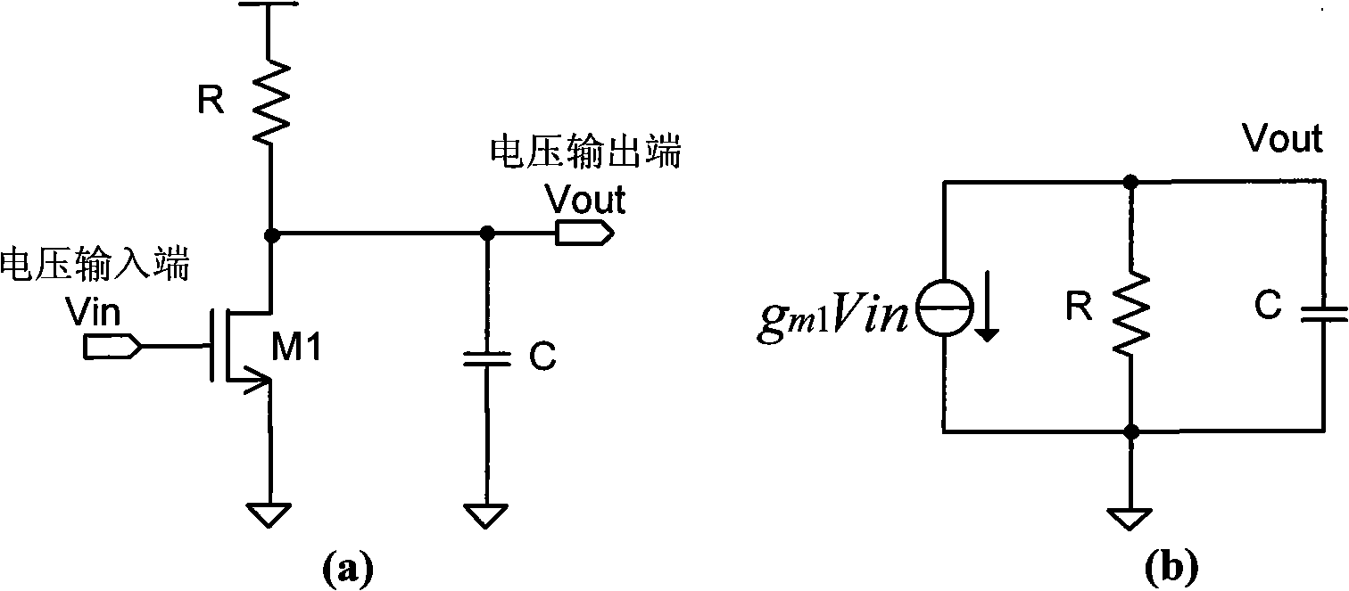
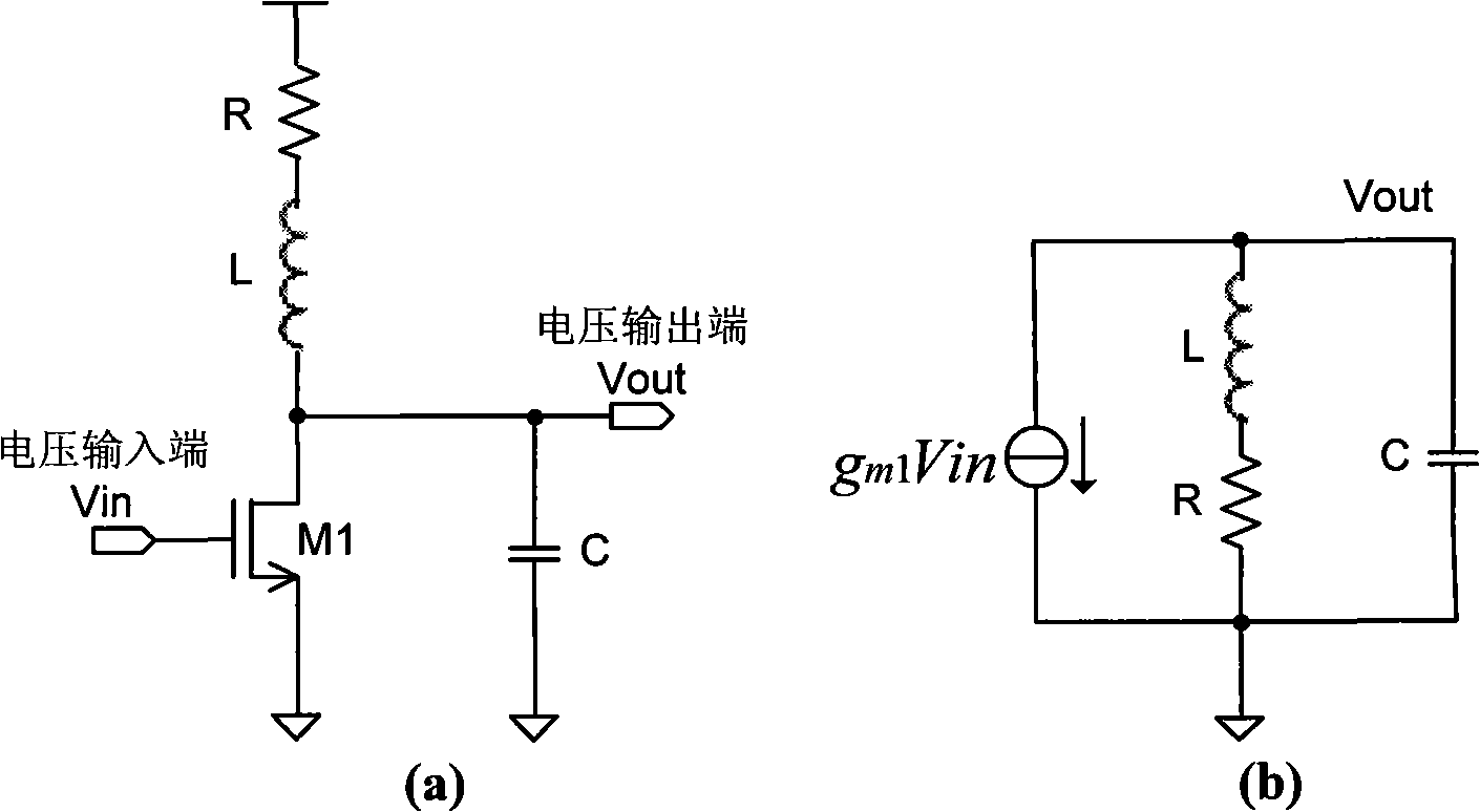
[0046] First, review figure 1 , figure 2 and Figure 5 The transient response process of the circuit. Explain the design idea of ​​the invention.

[0047] exist figure 1 When the signal Vin at the input terminal of the voltage amplifying circuit changes, part of the AC current of the amplifying tube M1 comes from the load resistance R, and the other part comes from the parasitic capacitance C at the output terminal. Due to the shunt effect of the resistor, only a part of the AC current of M1 is used for The charging and discharging of the parasitic capacitor C causes the output terminal voltage Vout to change slowly, and the signal conversion time is long.

[0048] exist figure 2 In the shown voltage amplifying circuit using a passive inductance parallel peaking structure, since the current of the inductance in the load impeda...


PUM


Abstract

The invention discloses an active inductance parallel peaking structure which is characterized by comprising a load impedance circuit and a load impedance current control circuit, wherein the load impedance circuit is used for converting current from a transconductance circuit into circuit output voltage; the load impedance current control circuit is used for carrying out time domain delay and frequency domain low-pass filtering processing on the voltage of an output end of the load impedance circuit and electric potential translational and additional processing; the output end of the load impedance circuit is connected with an input end of the load impedance current control circuit; and an output end of the load impedance current control circuit is connected with an input end of the load impedance circuit.

Description

technical field [0001] The invention relates to a semiconductor integrated circuit, in particular to an Active Inductor Shunt Peaking structure for high-speed analog voltage signal amplification circuits, broadband data communication circuits and high-speed digital circuits. Background technique [0002] The finite characteristic frequency of semiconductor transistors and the -3dB frequency ω of circuits -3dB , is the main reason for limiting the speed of integrated circuits. With the development of semiconductor technology, the characteristic frequency of transistors has been greatly improved, so increasing the -3dB frequency from the circuit topology has become the key to improving the working speed of integrated circuits. [0003] To illustrate the effect of the -3dB frequency on the speed of the circuit, in figure 1 In (a), the common-source amplifier circuit with load impedance adopting resistance R is given, in which the NMOS transistor M1 is an amplifier tube, which...

Claims


Application Information

Patent Timeline
Patent Type & Authority Applications(China)
IPC IPC(8): H03H11/50
Inventor 汪西虎吴龙胜刘佑宝
Owner CHINA AEROSPACE TIMES ELECTRONICS CORP NO 771 RES INST
Why Eureka
Try Eureka