Processing method of ultra-thin core board in manufacturing of printed circuit board or integrated circuit package substrate

A technology for printed circuit boards and integrated circuits, which is applied in the direction of multi-layer circuit manufacturing, circuits, and electrical components. , the effect of improving production efficiency and yield

Active Publication Date: 2009-09-23
SHANGHAI MEADVILLE SCI & TECH
View PDF0 Cites 29 Cited by
  • Summary
  • Abstract
  • Description
  • Claims
  • Application Information

AI Technical Summary

Problems solved by technology

In order to reduce the overall thickness of the circuit board and substrate after completion, when the dielectric layer of the core board is thin, such as as low as below 50um, special and expensive ultra-thin core board processing equipment must be used for processing, and the production cost will increase significantly
The industry also adopts the frame on the vertical production line and the method of using the guide plate on the horizontal production line to process ultra-thin core boards on conventional equipment to avoid problems such as bending, breaking or jamming, but these methods have complex operations and high efficiency. And the disadvantages of low yield

Method used


Image

  • Processing method of ultra-thin core board in manufacturing of printed circuit board or integrated circuit package substrate
  • Processing method of ultra-thin core board in manufacturing of printed circuit board or integrated circuit package substrate
  • Processing method of ultra-thin core board in manufacturing of printed circuit board or integrated circuit package substrate

Examples


Embodiment 1

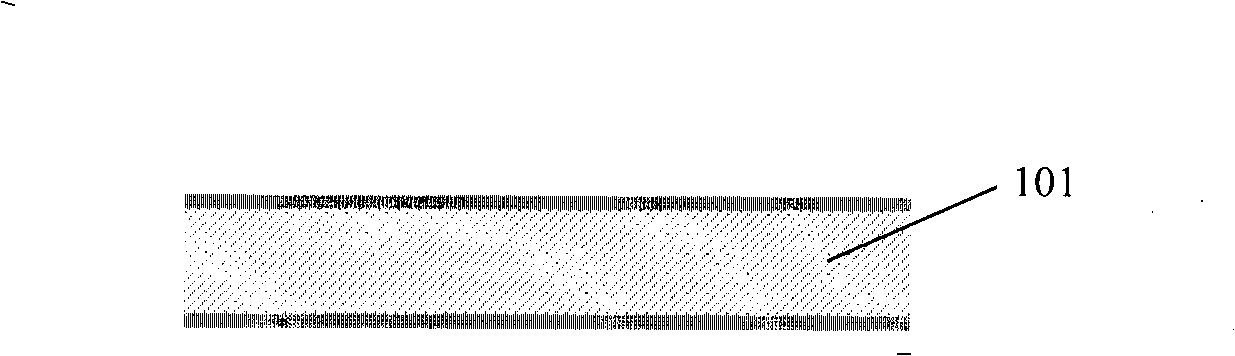
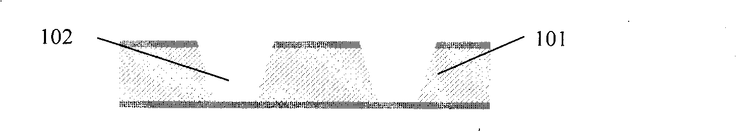
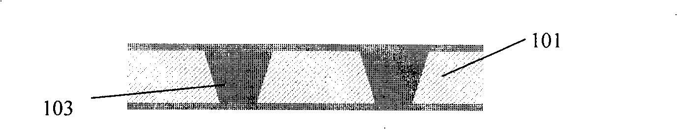
[0056] Figure 2-13 The printed circuit board or semiconductor integrated circuit package substrate of any interlayer interconnection made for the present invention, wherein, 207 is a conductor pattern, 205 is a solid conductive microhole, 208 is an insulating dielectric material formed by a build-up method, 201 Ultra-thin core board used in the initial stage of the method of the present invention.

[0057] The main manufacturing process of any interlayer interconnection printed circuit board or semiconductor integrated circuit packaging substrate of the present invention is as follows:

[0058] The production process is as follows:

[0059] In the first step, two ultra-thin core boards A1, A2 (201, 201'), two copper foils 203 and bonding sheets 202 are Figure 2-2 The structure is stacked, and then they are bonded together by hot pressing to form a multi-layer processed board B1. Figure 2-3 As shown; according to the thickness of the core board and the requirements for th...

Embodiment 2

[0070] Figure 3-9 Another printed circuit board or semiconductor integrated circuit packaging substrate made for the present invention, wherein, 207 is a conductor circuit pattern, 205 is a solid conductive microhole, 208 is an insulating dielectric material formed by a lamination method, and 201 is a circuit pattern of the present invention. In the ultra-thin core board used in the initial stage of the method, 212 is a mechanical through hole, and 213 is a mechanical buried hole.

[0071] The production process is as follows:

[0072] In the first step, two ultra-thin core boards A1, A2 (201, 201'), two copper foils 203 and bonding sheets 202 are Figure 3-1 The structure is stacked, and then hot pressing is used to bond them together to form a multi-layer processed board B1; select the appropriate adhesive according to the thickness of the core board and the hardness and strength requirements of the laminated multi-layer processed board B1 The junction sheet 202, in this ...


PUM


Abstract

A processing method of thin core board in manufacturing of printed circuit board or integrated circuit package substrate comprises the followings: copper foil and bonding sheet, two core boards are used for laminating and thermocompression bonding to obtain a processing board with periphery being bonded, and the thickness and strength thereof can satisfy the processing requirements of conventional devices; pattern conversion processing is carried out on the bonded processing board; laminating method is carried out on newly formed conductor line pattern surface, insulating medium and conductor line are formed through laminating, laser beam drilling, plating and pattern conversion technology; the previous processes are repeated to form multilayer processing boards; when two sides of multilayer processing boards reaches certain thickness and strength, the multilayer processing boards are incised at the bonding joint to form two processing boards; conventional laminating, drilling, plating and pattern conversion technologies are adopted to process the two processing boards respectively until the manufacturing of the needed circuit board and package substrate is finished. The invention needs no special device or processing tool to process thin core board, thus greatly reducing cost and improving productivity and yield of the product.

Description

technical field [0001] The invention relates to a processing method of an ultra-thin core board in the production process of a printed circuit board or a semiconductor integrated circuit packaging substrate, and the method is especially suitable for processing a printed circuit board or a semiconductor integrated circuit packaging substrate containing any layer interconnection make. Background technique [0002] With the vigorous development of the electronic industry, electronic products have entered the stage of functional and intelligent research and development. In order to meet the development needs of high integration, miniaturization and miniaturization of electronic products, printed circuit boards or semiconductor integrated circuit packaging substrates are used in Under the premise of satisfying the good electrical and thermal performance of electronic products, it is also developing towards the design trend of light, thin, short and small, so as to reduce the size...

Claims


Application Information

Patent Timeline
Patent Type & Authority Applications(China)
IPC IPC(8): H05K3/46H01L21/48
Inventor 罗永红吴金华
Owner SHANGHAI MEADVILLE SCI & TECH
Why Eureka
Try Eureka