Detection method for diffused junction of InGaAs/InP plane type photoelectric detector

A technology of photodetector and detection method, applied in electromagnetic measurement device, electric/magnetic depth measurement, measurement of resistance/reactance/impedance, etc., can solve the measurement conditions that are susceptible to corrosion defects, large errors, and it is difficult to accurately determine the PN junction problems such as the location of the junction area, to achieve the effect of convenient implementation and obvious characteristics of the junction area

Inactive Publication Date: 2009-09-30
SHANGHAI INST OF TECHNICAL PHYSICS - CHINESE ACAD OF SCI
View PDF0 Cites 8 Cited by
  • Summary
  • Abstract
  • Description
  • Claims
  • Application Information

AI Technical Summary

Problems solved by technology

Among them, the SIMS method measures the concentration distribution of p-type impurities in the depth direction of the material, and the impurity concentration generally changes gradually at the diffusion front, so it is difficult to accurately determine the position of the junction region of the PN junction; the ECV method can sense the depth distribution of carriers, and the spatial resolution It can reach the nanometer level, but it is easily affected by corrosion defects and measurement conditions; and the ECV method is only suitable for the measurement of carrier distribution of bulk materials, and cannot be applied to the detection of specified diffusion windows or photosensitive units of submillimeter or even micron size ; The commonly used SIMS method will also produce large errors when used for the measurement of impurity distribution with a window or photosensitive element size smaller than 100 microns
In addition, neither of the above two methods can provide information on the lateral diffusion of impurities.

Method used


Image

  • Detection method for diffused junction of InGaAs/InP plane type photoelectric detector
  • Detection method for diffused junction of InGaAs/InP plane type photoelectric detector
  • Detection method for diffused junction of InGaAs/InP plane type photoelectric detector

Examples


Embodiment 1

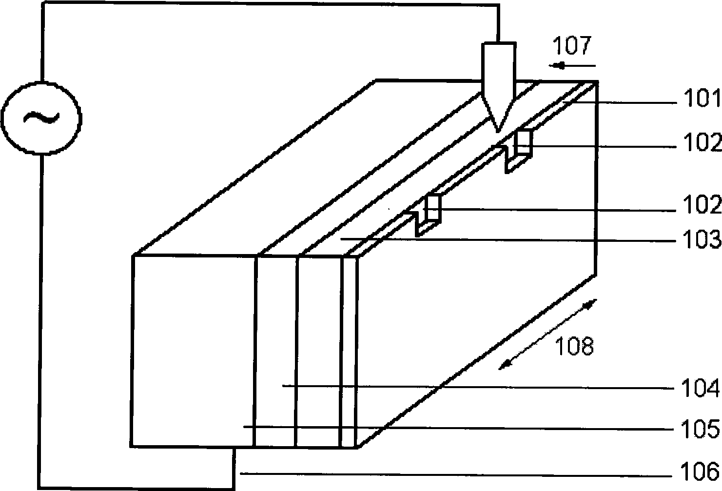
[0046] Embodiment 1 provides an InGaAs / InP avalanche photodiode (APD) diffusion junction, the avalanche photodiode structure at least includes a substrate, a bottom electrode, a photosensitive layer, a gradient layer, an electric field control layer, and a multiplication layer and a top electrode; the bottom electrode is above the substrate, which is n-type InP; the photosensitive layer is above the bottom electrode layer, which is non-doped i-InGaAs; the graded layer is above the photosensitive layer, which is composition gradient InGaAsP; electric field control The layer is above the graded layer, which is n-type InP; the multiplication layer is above the electric field control layer, which is non-doped i-InP; the top electrode layer is partially diffused by Zn impurities from the non-doped i-InP layer to form a p-type region.

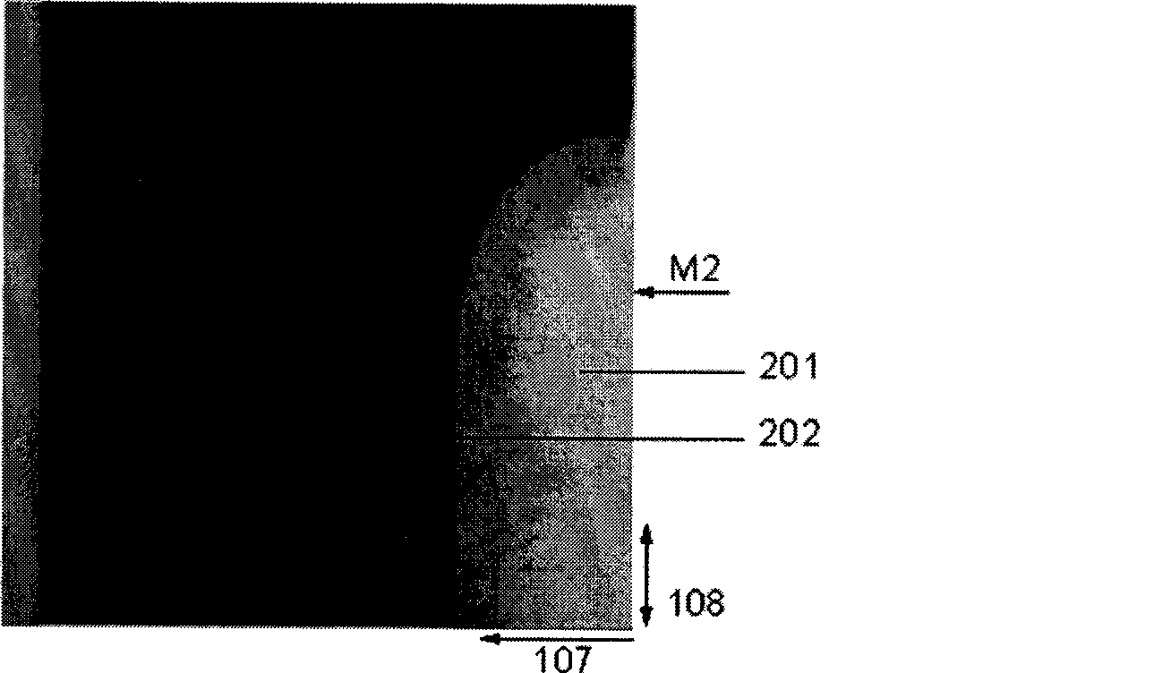
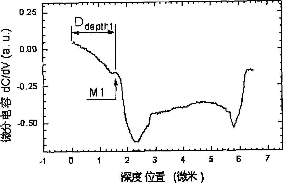
[0047] After obtaining the n-type common electrode and a flat and smooth cleavage section according to the above methods and steps, the differential ...

Embodiment 2

[0050] Embodiment 2 provides a kind of InGaAs / InP near-infrared PIN photodetector diffusion junction, this PIN photodetector structure at least comprises a substrate, a bottom electrode, a photosensitive layer, a top electrode; Wherein the bottom electrode is between the substrate The upper part is n-type InP; the photosensitive layer is above the bottom electrode layer, which is non-doped i-InGaAs; the top electrode layer is above the photosensitive layer, which is non-doped i-InP, which is partially diffused by Zn impurities to form a p-type region.

[0051] The sample preparation of embodiment 2 device structure diffusion junction detection is the same as that of embodiment 1, Figure 5 is the measured differential capacitance distribution of the cleavage surface. It can be seen from the figure that the p-type diffusion region has entered the InGaAs photosensitive layer, and the lateral diffusion speed of Zn impurities in the InGaAs layer is significantly faster than that of...


PUM


Abstract

The invention discloses a detection method for a diffused junction of an InGaAs/InP plane type photoelectric detector. The detection method comprises the following steps: carrying out the sectional plane sample preparation when a wafer or device to be tested passes through a diffusion zone; carrying out the sensing of the micro-distribution of differential capacitance in the diffusion zone and near zones on the sectional plane; and determining the position and diffusion depth of a PN junction according to the micro-distribution characteristic of the differential capacitance. The method is suitable for the detection of a small-size diffusion window and a photosensitive unit of the plane type photoelectric detector, has high spatial discrimination, and can provide information on lateral diffusion depth.

Description

technical field [0001] The invention relates to a detection method of a semiconductor element, in particular to a detection method of a diffusion junction of an InGaAs / InP planar photodetector. Background technique [0002] Semiconductor photodetectors are sensing devices that realize photoelectric information conversion. In the near-infrared band (wavelength of light: 1-3 microns), InGaAs / InP has become the main application material for photodetectors in this band because of its excellent material properties. The InGaAs / InP detector structure is mainly divided into two types: planar type and mesa type; among them, the planar type structure avoids the factors affecting the photoelectric efficiency such as leakage and surface recombination caused by the side wall of the mesa device, and can obtain better detection performance, so It is widely used in two main photodetectors of InGaAs / InP: avalanche photodiode (APD) and PIN near-infrared detector. The preparation of the PN j...

Claims


Application Information

Patent Timeline
Patent Type & Authority Applications(China)
IPC IPC(8): G01N27/22G01R27/26G01B7/26
Inventor 李天信陆卫殷豪李永富王文娟唐恒敬李宁李志峰陈效双龚海梅
Owner SHANGHAI INST OF TECHNICAL PHYSICS - CHINESE ACAD OF SCI
Why Eureka
Try Eureka