Liquid crystal display panel structure and manufacturing method thereof

A technology of liquid crystal display and manufacturing method, which is applied in the directions of instruments, nonlinear optics, optics, etc., can solve the problems of uneven cell thickness around the liquid crystal display panel, unable to maintain a proper gap between glass substrates, and glass spacers gathering together, etc. Achieve the effect of improving display quality, good support strength and conductivity, good support strength and conductivity

Active Publication Date: 2009-09-30
K TRONICS (SUZHOU) TECH CO LTD +1
View PDF0 Cites 17 Cited by
  • Summary
  • Abstract
  • Description
  • Claims
  • Application Information

AI Technical Summary

Problems solved by technology

In the process of realizing the above-mentioned solution 1, the inventors found that there are at least the following problems in the prior art: since the conductive glue is point-connected, the upper and lower substrates can only achieve electrode conduction through the point where the conductive glue is located, which is not conducive to the connection between charges. Moreover, since the conductive adhesive occupies a certain position, the fluctuation range of the position of the sealing glue is reduced, and the defect rate of the product increases to a certain extent; in addition, the metal at the position of the conductive adhesive is easily corroded
[0007] In the process of realizing the above two solutions, the inventor found at least the following problems in the prior art: the glass spacer is mixed in the frame sealant, mainly to support the upper and lower glass substrates, and it must be evenly distributed with the sealant. The frame glue is coated on the glass substrate, once the distribution is uneven, it will cause some glass spacers to gather together
In the whole process, it is easy to cause the glass spacer to be unevenly distributed in the sealant and gather together, resulting in uneven thickness of the surrounding box of the LCD panel, resulting in defects, and it is impossible to maintain the upper and lower glass substrates. Appropriate gaps between them will cause uneven distribution of the electric field, resulting in partial or overall unevenness of the screen, which will affect the display quality of the product; in addition, the conductive balls in the second scheme will also appear in the uneven distribution of the sealing glue , affecting the conduction of current between the two substrates, which in turn affects the display quality of the product

Method used


Image

  • Liquid crystal display panel structure and manufacturing method thereof
  • Liquid crystal display panel structure and manufacturing method thereof
  • Liquid crystal display panel structure and manufacturing method thereof

Examples


Embodiment Construction

[0033] The present invention will be described in further detail below in conjunction with the accompanying drawings.

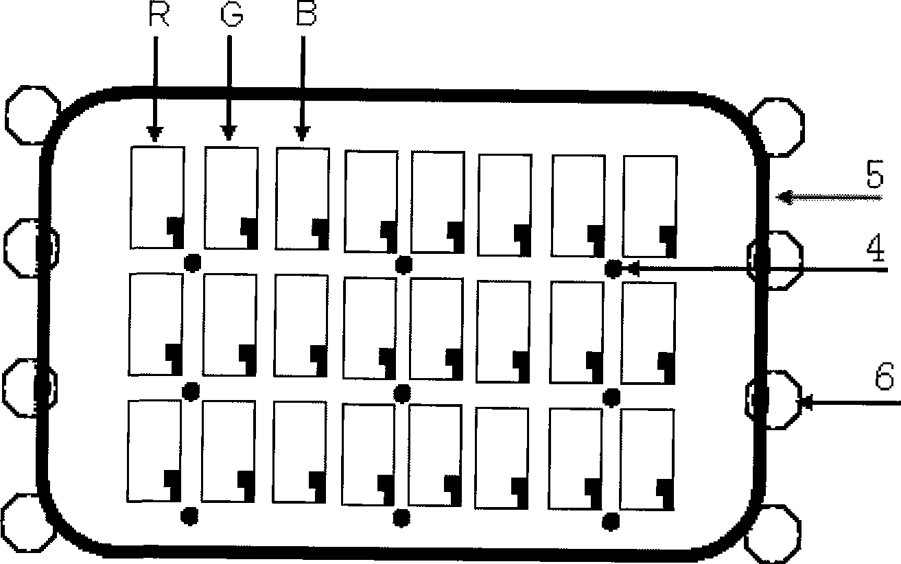
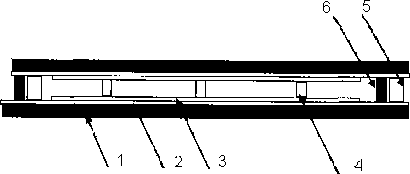
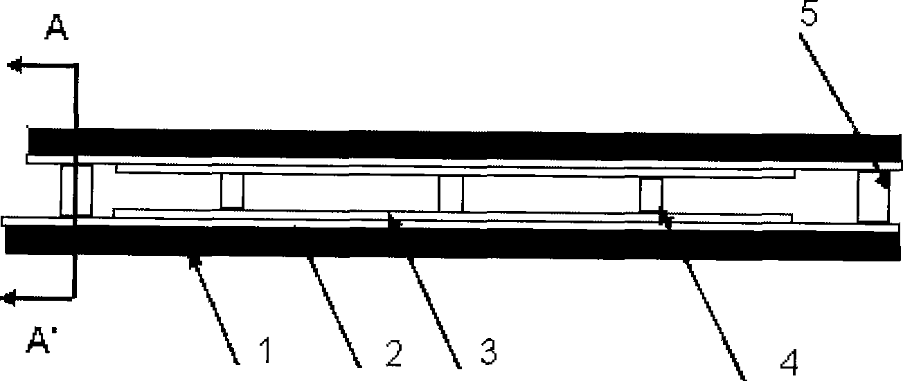
[0034] In order to solve the problem of poor display quality of the liquid crystal display panel in the prior art, the present invention provides a liquid crystal display panel. Such as Figure 5 , Figure 6 As shown, the liquid crystal display panel includes: a color filter substrate and an array substrate disposed opposite to each other, support spacers 4 are evenly distributed in the display area on the side of the color filter substrate opposite to the array substrate, and the color filter substrate is opposite to the array substrate. The edge of one side is bonded to the edge of the array substrate opposite to the color filter substrate through the sealant 5 to form a closed area, and the closed area is filled with liquid crystals.

[0035] In order to provide good support strength and electrical conductivity between the color filter substrate and the ...


PUM


Abstract

The invention discloses a liquid crystal display panel structure and a manufacturing method thereof, belonging to the technical field of the liquid crystal displays and being invented aiming to improve the display quality of the liquid crystal display. The liquid crystal display panel structure comprises a color film substrate and an array substrate which are oppositely arranged, supporting spacers are evenly distributed in a display area at one side of the color film substrate relative to the array substrate, the edge at one side of the color film substrate relative to the array substrate is stuck with the edge at one side of the array substrate relative to the color film substrate through frame sealing adhesive to form a closed area, and the closed area is filled with liquid crystals; a conducting spacer is arranged on the edge at one side of the color film substrate relative to the array substrate and is embedded in the frame sealing adhesive, and both ends of the conducting spacer are respectively in contact with the two substrates to realize the electric connection between the two substrates; and the conducting spacer has good supporting strength and good electric conductivity. The invention is suitable for improving the display quality of the liquid crystal display.

Description

technical field [0001] The invention relates to the technical field of liquid crystal displays, in particular to a liquid crystal display panel structure and a manufacturing method thereof. Background technique [0002] At present, with the development of science and technology, thin film transistor liquid crystal display (TFT-LCD) has become the mainstream product of information display due to its advantages of excellent display quality and reasonable price. Optimization. [0003] The liquid crystal display panel consists of upper and lower glass substrates: the upper glass substrate is a color filter substrate, which carries a color filter film (CF, Color Filter) displaying RGB three primary colors; the lower glass substrate is an array substrate, which is an array of TFT control switches . In the production process of liquid crystal display panels, the sealing of the array substrate and the color filter substrate and the current conduction between the two substrates are...

Claims


Application Information

Patent Timeline
Patent Type & Authority Applications(China)
IPC IPC(8): G02F1/1339G02F1/1333
Inventor 赵承潭陈永张莹
Owner K TRONICS (SUZHOU) TECH CO LTD
Why Eureka
Try Eureka