Method for preparing ZnO nanorods array
A technology of nanorod array and seed layer is applied in the field of preparation of ZnO nanorod array, which can solve the problems of uneven distribution and large difference in size of ZnO nanorods, and achieve the effect of improving product quality and shortening preparation time.
- Summary
- Abstract
- Description
- Claims
- Application Information
AI Technical Summary
Problems solved by technology
Method used
Image
Examples
Embodiment Construction
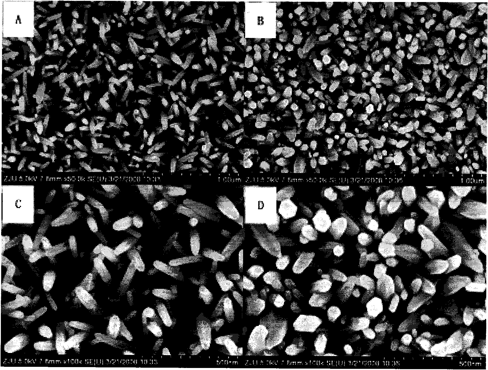
[0010] The preparation method of the ZnO nanorod array of the present invention is firstly the preparation of the dielectric layer. The silicon wafer selected as the substrate is cleaned and placed in a high-temperature furnace for thermal oxidation. After thermal oxidation at a temperature of 1140 ° C for 40 minutes, A 50nm thick silicon dioxide layer is grown on the surface of the substrate.
[0011] Then a 100nm-thick Zn film was deposited on the dielectric layer of the silicon substrate by means of DC magnetron sputtering, before which the substrate was cleaned by plasma bombardment. When depositing Zn film, the purity of the zinc target is 99.999%, the diameter of the zinc target and the distance between the target and the substrate are 6cm, and the background vacuum is 1.6×10⁻⁴Pa. High-purity argon is introduced through a flow control system. The working pressure in sputtering was kept at 1.0 Pa. The sputtering power was 50W, and the time lasted 20min. Under atmospher...
PUM
 Abstract
Description
Claims
Application Information
