
Mold framework and liquid crystal display device

A frame and outer frame technology, applied in nonlinear optics, instruments, optics, etc., can solve problems such as reduced service life, SR layer shedding of COF film, short circuit of data lines, etc., to improve life, reduce friction, and avoid shedding Effect

Active Publication Date: 2009-10-07
BOE TECH GRP CO LTD +1
View PDF3 Cites 12 Cited by
  • Summary
  • Abstract
  • Description
  • Claims
  • Application Information

AI Technical Summary

Problems solved by technology

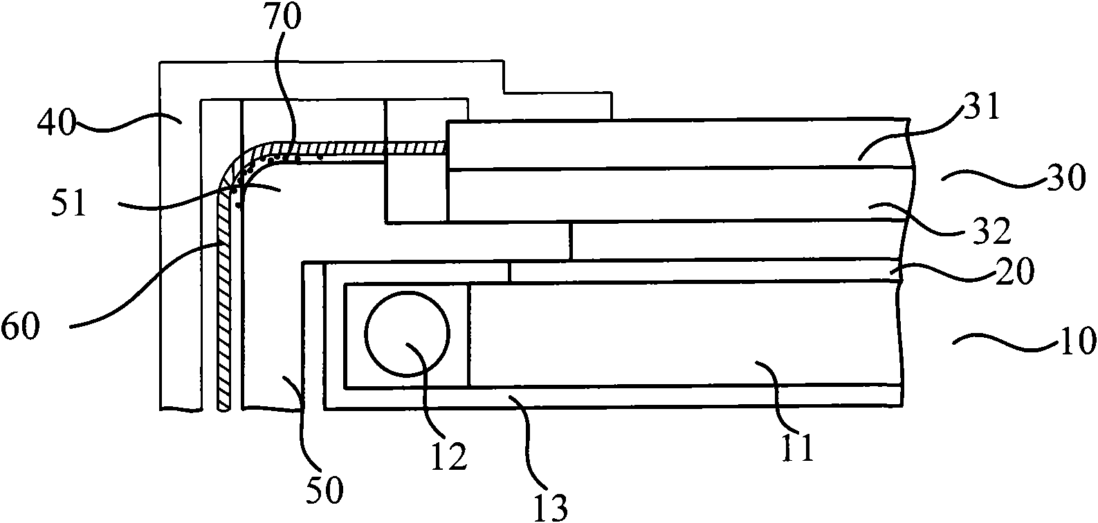
[0003] However, the defect of the liquid crystal display device with the above structure is that some corners of the liquid crystal display device outer frame 40 will be rubbed against parts such as the backlight plate 13, thereby generating metal debris 70, especially aluminum flakes (AL chip)
The position where the metal debris 70 is easy to spread out, that is, the notch 51 where the fixed drive line 60 is embedded on the mold frame 50, is also called the COF (Chips On Film, COF for short) contact surface, and a large amount of metal will accumulate on it. chips 70, so there will be friction cutting between COF and M / F, such as figure 1 As shown, causing the SR layer of the COF film to peel off
Therefore, the floating metal debris 70 will cause a short circuit of the data line at the place where the SR layer of the COF falls off, causing the liquid crystal display device to malfunction and reduce its service life.

Method used


Image

  • Mold framework and liquid crystal display device
  • Mold framework and liquid crystal display device
  • Mold framework and liquid crystal display device

Examples


Embodiment Construction

[0021] Mold frame embodiment one

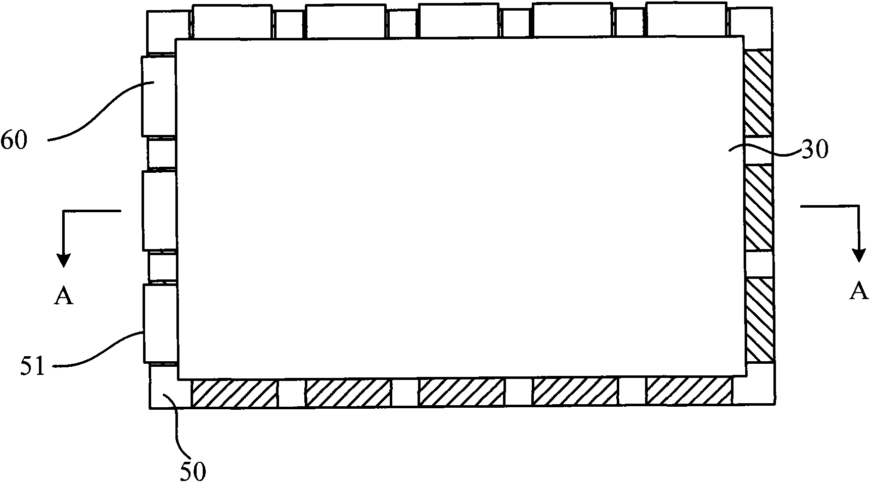
[0022] Such as image 3 Shown is a partial top view structure schematic diagram of a specific embodiment 1 of the mold frame of the present invention, and the mold frame 50 can be specifically applied to a liquid crystal display device to play a role of support and protection. The mold frame 50 is a rectangular frame, on which several notches 51 for accommodating the driving circuit of the liquid crystal display device are provided at intervals, and each notch 51 is provided with grooves 52 arranged in a matrix form, image 3 It is an enlarged schematic view of the structure of one of the notches 51 , and the cross-sectional shape of the notch 52 is a rectangle.

[0023] After the mold frame of this embodiment is placed into the liquid crystal display device, such as Figure 4 As shown, on the one hand, since the notch 51 is provided with a groove 52, the contact area between the data drive chip and the data line connection part (COF) and t...


PUM

PropertyMeasurementUnit
Diameteraaaaaaaaaa

Abstract

The invention relates to a mold framework and a liquid crystal display device. A plurality of notches for containing and embedding driving lines are arranged on the mold framework at intervals, wherein a plurality of projections and / or grooves are arranged on each notch. The liquid crystal display device adopts the mold framework of the invention and further comprises: a backlight module, an optical film layer and a panel which are sequentially arranged from bottom to top, as well as an external framework which is surrounded at the outside of the backlight module, the optical film layer and the panel, wherein the mold framework is embedded between the external framework and the backlight module and between the optical film layer and the panel, and the driving lines connected on the panel are embedded in the notches of the mold framework. The invention reduces the contact area of the driving lines with the mold framework, reduces the friction occurred on the contact surface, avoids theshedding phenomenon of an SR layer, plays the role of collecting metal debris, further avoids the short-circuit phenomenon of a data cable caused by the adhesion of the metal debris on COF and can improve the service life of the liquid crystal display device.

Description

technical field [0001] The invention relates to a mold frame and a liquid crystal display device, in particular to a mold frame applied to a liquid crystal display device and a liquid crystal display device equipped with the mold frame. Background technique [0002] The liquid crystal display device is one of the commonly used flat panel display devices at present. Taking Thin Film Transistor-Liquid Crystal Display (hereinafter referred to as TFT-LCD) as an example, its basic structure is as follows: figure 1 As shown, it usually includes a backlight module 10 (BlackLight Unit, hereinafter referred to as BLU), an optical film layer 20 (sheet), a color filter substrate 31 (CF) and an array substrate 32 (Array) that are arranged from bottom to top. The panel 30 (panel) also includes a mold frame 50 (moldframe, referred to as M / F) that is arranged on the side of the backlight module 10, the optical film layer 20 and the panel 30, and plays a role of fixing and supporting, and i...

Claims


Application Information

Patent Timeline
IPC IPC(8): G02F1/1333
Inventor 李相稙尹大根金哲润
Owner BOE TECH GRP CO LTD
Learn More