Device and method for testing wireless baseband chips in base station side

A test device and wireless-based technology, applied in wireless communication, transmission monitoring, electrical components, etc., can solve problems such as difficulty in judging whether the chip under test is working normally or not, and achieve the effect of alleviating the demand for a large number of testing instruments and saving R&D costs

Active Publication Date: 2009-10-14
SANECHIPS TECH CO LTD
View PDF0 Cites 20 Cited by
  • Summary
  • Abstract
  • Description
  • Claims
  • Application Information

AI Technical Summary

Problems solved by technology

[0009] The technical problem to be solved by the present invention is to provide a base station side wireless baseband chip testing device and method, which can solve the problem that it is difficult to determine whether the chip to be tested is working normally or not based on the test results of the whole machine using traditional testing methods

Method used


Image

  • Device and method for testing wireless baseband chips in base station side
  • Device and method for testing wireless baseband chips in base station side
  • Device and method for testing wireless baseband chips in base station side

Examples


Embodiment Construction

[0041] The technical solution of the present invention will be explained in detail below in conjunction with the accompanying drawings and specific embodiments.

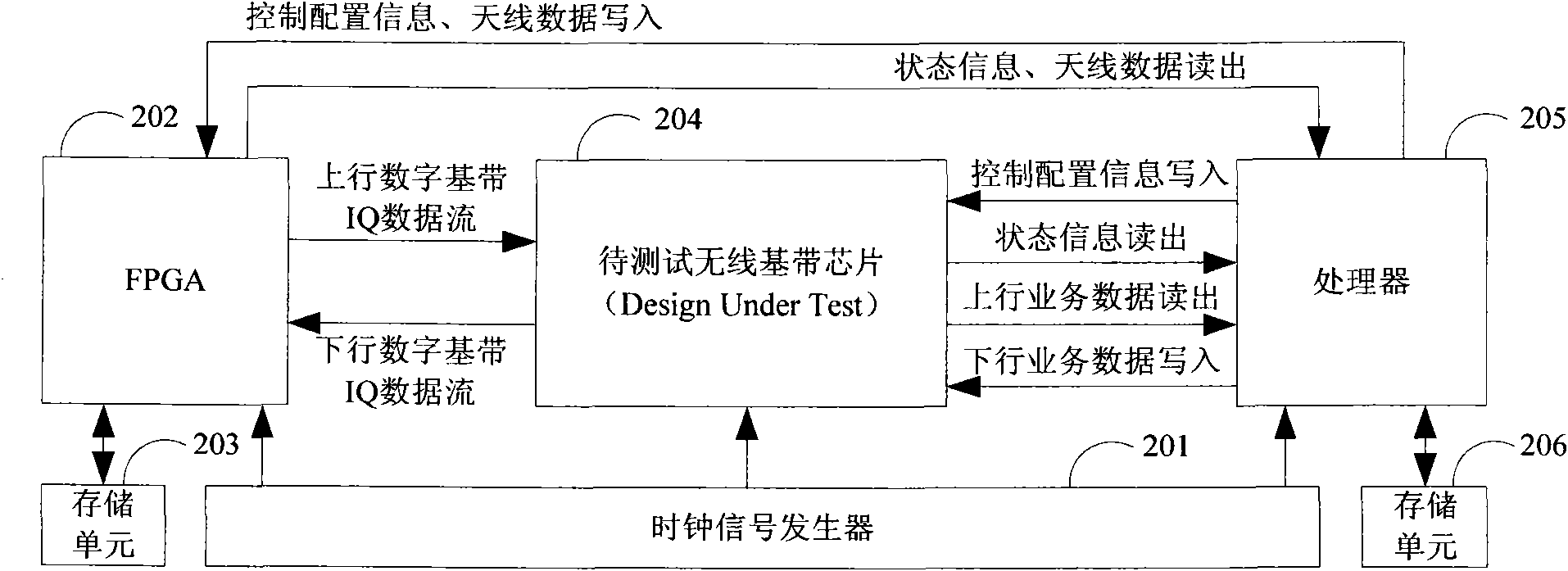
[0042] figure 2 A schematic structural diagram of an embodiment of the base station side wireless baseband chip reliability testing device of the present invention is provided, the device includes: a clock signal generator 201, a field programmable logic array FPGA202 and a storage unit 203 attached thereto, a wireless device to be tested The baseband chip 204, the processor 205 and the storage unit 206 attached thereto; wherein:

[0043] Clock signal generator 201 is connected with FPGA 202, wireless baseband chip 204 to be tested and processor 205 respectively, and is used to provide them with correct clock, reset signal and timing signal, so that each functional unit has correct input clock and can be Reliably reset and synchronized on timing to work well together.

[0044]The FPGA 202 is connected to the stora...


PUM


Abstract

The invention relates to a device for testing wireless baseband chips in a base station side, which comprises mutually connected chips to be tested and a controller unit, wherein the chips to be tested are used as uplink and downlink tested objects, and the controller unit controls the generation of the data stream of an uplink antenna of the chips to be tested or collects the data stream of a downlink antenna of the chips to be tested at a right time point. The method comprises the steps: inquiring the state of the chips to be tested, reading uplink processing results output by the chips to be tested, comparing the uplink processing results with uplink parameter results, or comparing collected downlink antenna data streams with downlink parameter results, and inquiring the downlink operating state of the chips to be tested so as to respectively judge the correctness of the uplink processing results and the downlink processing results of the chips to be tested. The invention can make up the defect that a special wireless testing instrument can not achieve the function of bit-order calibration at a specified time point, alleviates the requirements of a plurality of sets of testing environments to a plurality of testing instruments and saves the costs of research and development.

Description

technical field [0001] The invention relates to digital integrated circuit design and testing technology in the field of wireless communication, in particular to a reliability testing device and method for a wireless baseband chip at a base station side in communication equipment. Background technique [0002] In the research and development process of the wireless baseband chip on the base station side, it is necessary to put the wireless baseband chip in the actual application system for reliability testing. Such as figure 1 A schematic diagram of a traditional base station equipment reliability test system is given. The whole test system includes: wireless terminal 101, wireless terminal 102, radio frequency equipment 103, reliability test environment 104, wireless baseband equipment 105, base station controller 106, core network 107, and the wireless baseband chip to be tested is placed in the wireless baseband equipment 105 , and the wireless baseband device 105 itsel...

Claims


Application Information

Patent Timeline
Patent Type & Authority Applications(China)
IPC IPC(8): H04W24/00H04B17/00H04B17/15H04B17/29
Inventor 许祥滨杨晓龙谭建华汤顺
Owner SANECHIPS TECH CO LTD
Why Eureka
Try Eureka