Optical spin injection method

A spin injection, optical technology, applied in sustainable manufacturing/processing, electrical components, climate sustainability, etc., can solve the problems of low spin polarization, low spin injection efficiency, low temperature operation only, etc. To achieve the effect of easy room temperature operation, practical application and easy integration

Inactive Publication Date: 2009-10-21
INST OF SEMICONDUCTORS - CHINESE ACAD OF SCI
View PDF0 Cites 11 Cited by
  • Summary
  • Abstract
  • Description
  • Claims
  • Application Information

AI Technical Summary

Problems solved by technology

The current injection method is to inject spins into semiconductors through ferromagnets, but this injection method results in very low spin injection efficiency due to the mismatch between the interface conductance of ferromagnetic metals and semiconductors; the spin Hall effect is used to generate spins. current, the disadvantage of this method is that it uses the spin-orbit coupling effect in semiconductors, so it is only suitable for narrow-bandgap semiconductors and can only be operated at low temperatures; Very low degree of spin polarization

Method used


Image

  • Optical spin injection method
  • Optical spin injection method
  • Optical spin injection method

Examples


Embodiment Construction

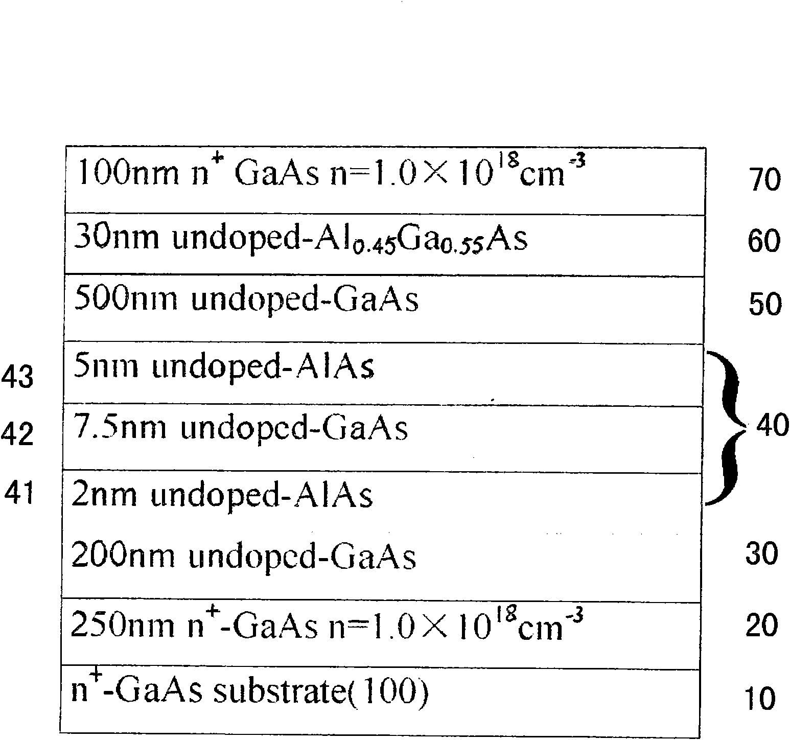
[0025] see figure 1 as shown, figure 1 It is a hierarchical structure diagram of materials involved in the present invention. Wherein a heavily doped GaAs substrate 10 is selected; a buffer layer 20 is grown on it, the thickness of the buffer layer 20 is 250nm, the material of the buffer layer 20 is heavily doped GaAs, and the buffer layer 20 can smooth the substrate, The subsequent growth of the epitaxial structure has fewer dislocations and a more complete lattice, ensuring its excellent optical and electrical properties. Then grow a layer of active layer 30, the thickness of the active layer 30 is 200nm, the material of the active layer 30 is GaAs, the inside of the active layer 30 can be embedded with quantum wells or quantum dots, to tunnel the self Spin manipulation of spin-polarized electrons. Thereafter, a layer of resonant tunneling structure 40 is grown, and the resonant tunneling structure 40 functions as a spin filter, so that the polarization degree of spin-pol...


PUM


Abstract

The invention relates to an optical spin injection method comprising the following steps: 1. a substrate is taken, and a buffer layer is grown on the substrate and used for smoothing the substrate to enable a following growing epitaxial structure to have high integrality; 2. an active layer is grown on the buffer layer and used for controlling spin polarized electrons; 3. a resonant tunneling structure is grown on the active layer and has a spin filtering function; 4. a light absorbing layer is grown on the resonant tunneling structure and used for generating the spin polarized electrons; 5. an electronic blocking layer is grown on the light absorbing layer and used for blocking and preventing non-spin polarized electrons; and 6. a heavily doped layer is grown on the electronic blocking layer and used for contacting ohm.

Description

technical field [0001] The invention relates to a spin injection method, in particular to introducing electrons with high spin polarization into semiconductor active regions by using optical polarization transfer and resonant tunneling. Background technique [0002] The continuous reduction of device size and the continuous improvement of integration density in CMOS integrated circuits have brought many problems. Quantum effects can no longer be ignored. The heat dissipation of devices and the yield rate of products all make Moore's Law, which is regarded as the golden rule, face huge challenges. At this time, people consider that using the spin of electrons is a good solution to the above problems. . [0003] The scale required by the spin-correlation effect is on the nanometer scale, which is an order of magnitude smaller than the tens of nanometers required by the charge, and the spin device is easier to achieve a higher degree of integration; secondly, the interaction o...

Claims


Application Information

Patent Timeline
Patent Type & Authority Applications(China)
IPC IPC(8): H01L31/18H01L31/111
CPCY02P70/50
Inventor 张飞郑厚植肖文波谈笑天孙晓明吴昊朱科罗晶
Owner INST OF SEMICONDUCTORS - CHINESE ACAD OF SCI
Why Eureka
Try Eureka