Method for incinerating etched substrate and method for forming etched structure

A technology of ashing and ashing treatment, applied in the direction of electrical components, semiconductor/solid-state device manufacturing, circuits, etc., can solve problems such as the etch stop layer that is easy to damage the lower layer, and achieve the effect of avoiding loss

Active Publication Date: 2009-11-04
SEMICONDUCTOR MANUFACTURING INTERNATIONAL (BEIJING) CORP
View PDF1 Cites 8 Cited by
  • Summary
  • Abstract
  • Description
  • Claims
  • Application Information

AI Technical Summary

Problems solved by technology

[0015] The invention provides a post-etching ashing method and a method for forming an etching structure, so as to improve the phenomenon that the etching stop layer of the lower layer is easily damaged during the existing post-etching ashing process, and improve the formation quality of the etching structure

Method used


Image

  • Method for incinerating etched substrate and method for forming etched structure
  • Method for incinerating etched substrate and method for forming etched structure
  • Method for incinerating etched substrate and method for forming etched structure

Examples


no. 1 example

[0084] The first embodiment of the present invention introduces a post-etching ashing method, Figure 4 is a flow chart of the post-etching ashing method according to the first embodiment of the present invention, Figure 5 to Figure 7 In order to illustrate the cross-sectional view of the device of the post-etch ashing method of the first embodiment of the present invention, the following is combined with Figure 4 to Figure 7 The first embodiment of the present invention will be described in detail.

[0085] Step 401: providing an etched substrate.

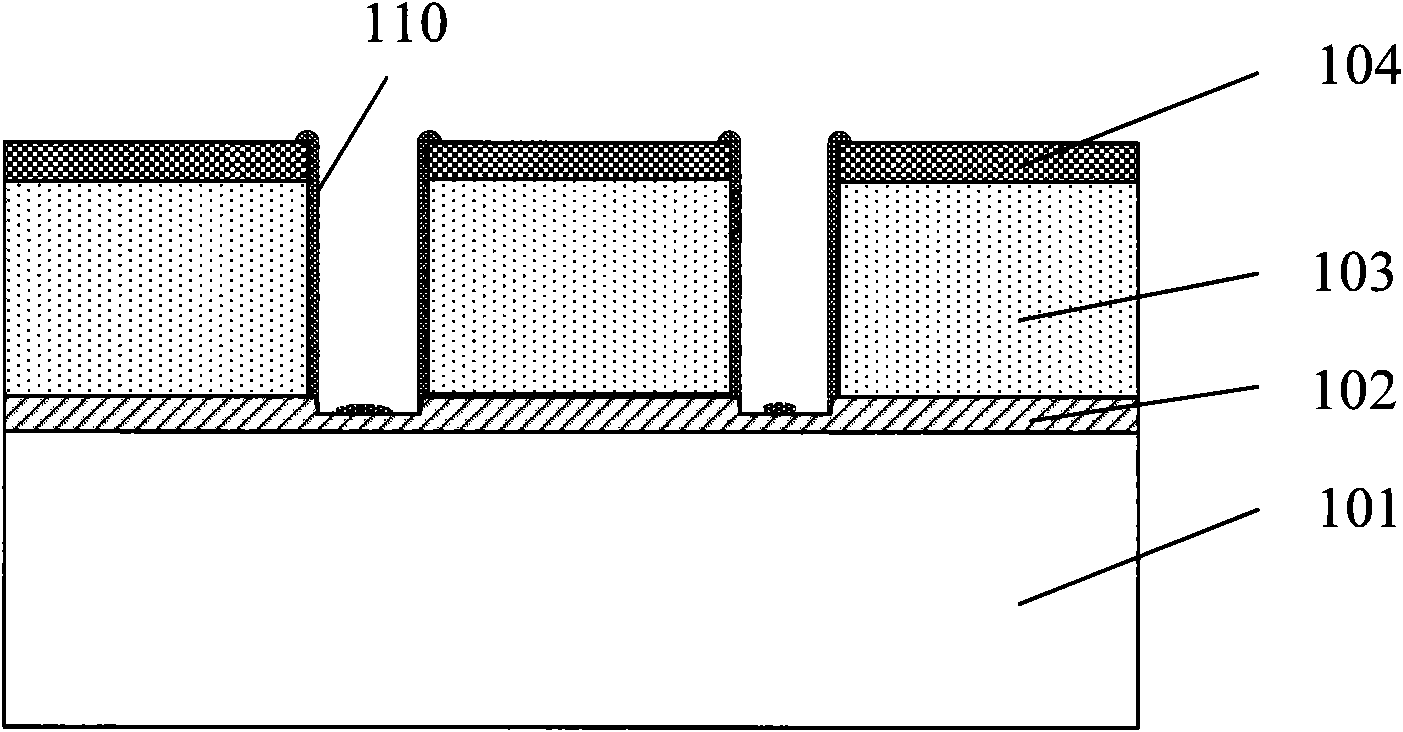
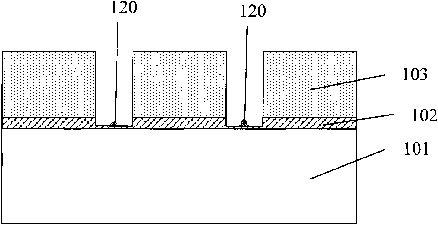
[0086] The etched substrate provided in this embodiment may be a substrate that has just been etched to form various etched structures (such as contact holes, through holes, dual damascene structures, etc.), and residual photoresist is still attached to its surface. and polymers.

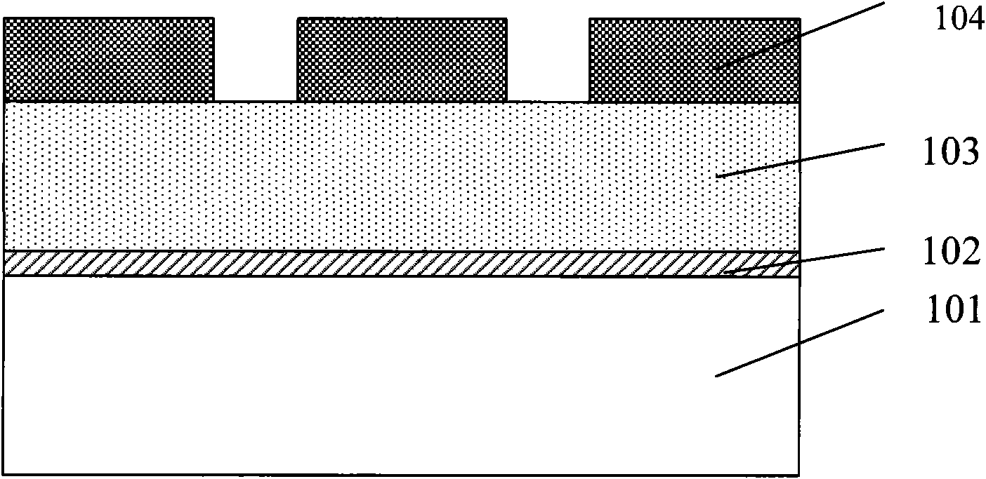
[0087] Figure 5 It is a schematic cross-sectional view of the etched substrate in the first embodiment of the present invention, as Figure 5 A...

no. 2 example

[0115] The second embodiment of the present invention introduces a method for forming an etching structure, Figure 10 It is a flow chart of the etching structure forming method according to the second embodiment of the present invention, Figure 11 to Figure 15 In order to illustrate the device cross-sectional view of the etching structure forming method of the second embodiment of the present invention, the following is combined with Figure 10 to Figure 15 The second embodiment of the present invention will be described in detail.

[0116] Step 1001: providing a substrate with a material layer to be etched on the substrate.

[0117] Figure 11 is a schematic cross-sectional view of the substrate in the second embodiment of the present invention, as Figure 11 As shown, a material layer 1104 to be etched is formed on a silicon substrate 1101. The material layer 1104 may be a silicon oxide layer, such as a phosphorus-containing silicon oxide layer, a black diamond layer, a...


PUM


Abstract

The invention discloses a method for incinerating an etched substrate, comprising the following steps: providing an etched substrate; putting the etched substrate in a processing chamber; guiding plasma gas into the processing chamber; incinerating the substrate for the first time by high radio frequency power supply; incinerating the substrate for the second time by low radio frequency power supply; and taking out the substrate. The invention also discloses a method for forming an etched structure with the method for incinerating the etched substrate. The method for incinerating an etched substrate and the method for forming an etched structure can ensure that the next layer of incinerated material is kept thick enough without thickening the next layer of material and narrowing an etching process window, thereby improving the quality of forming the etched structure.

Description

technical field [0001] The invention relates to the technical field of semiconductor manufacturing, in particular to an ashing method after etching and a method for forming an etching structure. Background technique [0002] The semiconductor manufacturing process is a planar manufacturing process that forms a large number of various types of complex devices on the same substrate and interconnects them to have complete electronic functions. In this manufacturing process, it is often necessary to form various patterns (structures) on the substrate by means of etching. At present, there is a problem of great concern in the formation process of this etching structure: the removal of the remaining photoresist and polymer (polymer) after etching. [0003] As the feature size of VLSI devices continues to scale down and the level of integration continues to increase, the requirements for etching technology that can completely copy mask patterns to the substrate surface are also ge...

Claims


Application Information

Patent Timeline
Patent Type & Authority Applications(China)
IPC IPC(8): H01L21/00H01L21/02H01L21/311G03F7/42
Inventor 孙武沈满华尹晓明
Owner SEMICONDUCTOR MANUFACTURING INTERNATIONAL (BEIJING) CORP
Why Eureka
Try Eureka