
Encapsulation structure and encapsulation method for modularization crystal grains

A packaging method and die technology, which are applied in the manufacturing of electrical components, electric solid-state devices, semiconductor/solid-state devices, etc., can solve the problems of reducing the reliability of the packaging structure, affecting the performance of the die, and damaging the die.

Active Publication Date: 2009-11-04
CHIPMOS TECH INC
View PDF2 Cites 4 Cited by
  • Summary
  • Abstract
  • Description
  • Claims
  • Application Information

AI Technical Summary

Problems solved by technology

The thinned die is redistributed on another substrate, and then multiple dies are formed into a package by injection molding; since the die is very thin, the package is also very thin, so when After the package is detached from the substrate, the stress of the package itself will cause the package to warp, increasing the difficulty of the subsequent cutting process
[0006] In addition, after the wafer is diced, when it is reconfigured on another carrier, since the size of the new carrier is larger than the original size, it will not be aligned in the subsequent ball planting process, and the reliability of the package structure will be reduced.
[0007] In addition, during the entire packaging process, there will be a problem that when the ball is planted, the manufacturing equipment will exert local excessive pressure on the die, which may damage the die; at the same time, it may also be caused by the material of the ball. The resistance value between the pads on the board becomes larger, which affects the performance of the grain and other issues

Method used


Image

  • Encapsulation structure and encapsulation method for modularization crystal grains
  • Encapsulation structure and encapsulation method for modularization crystal grains
  • Encapsulation structure and encapsulation method for modularization crystal grains

Examples


Embodiment Construction

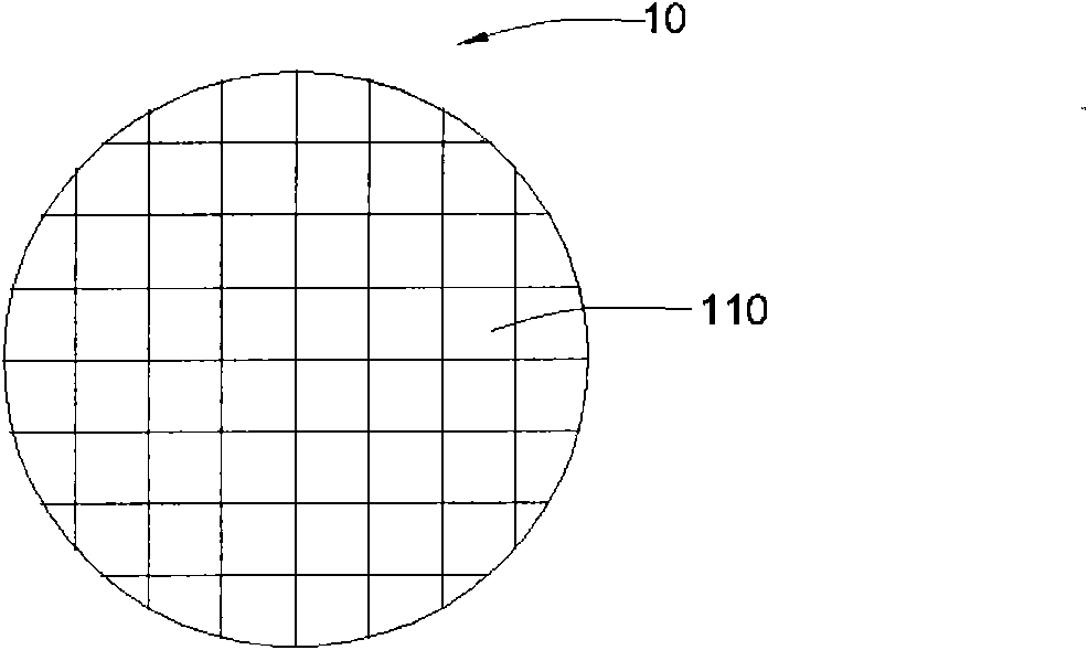
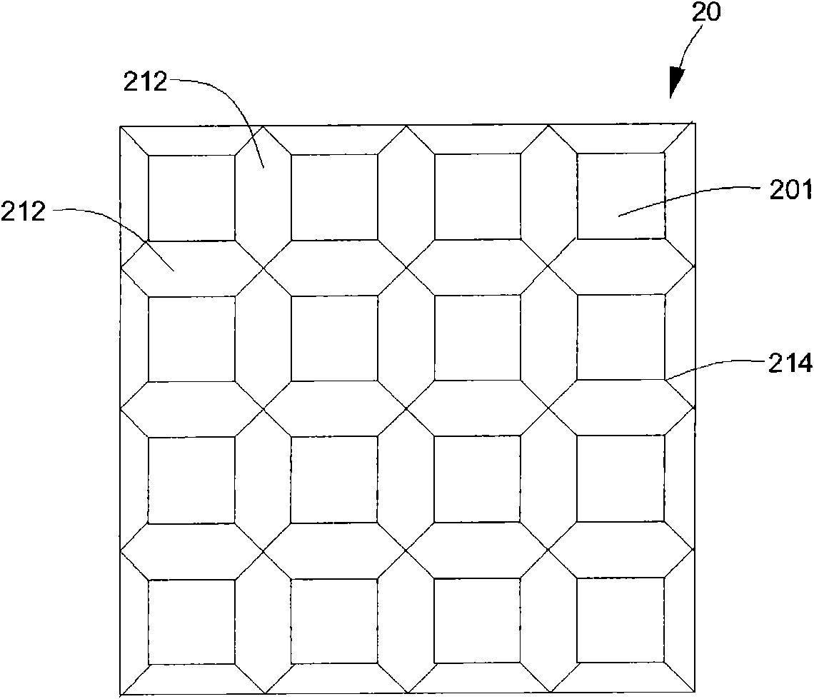
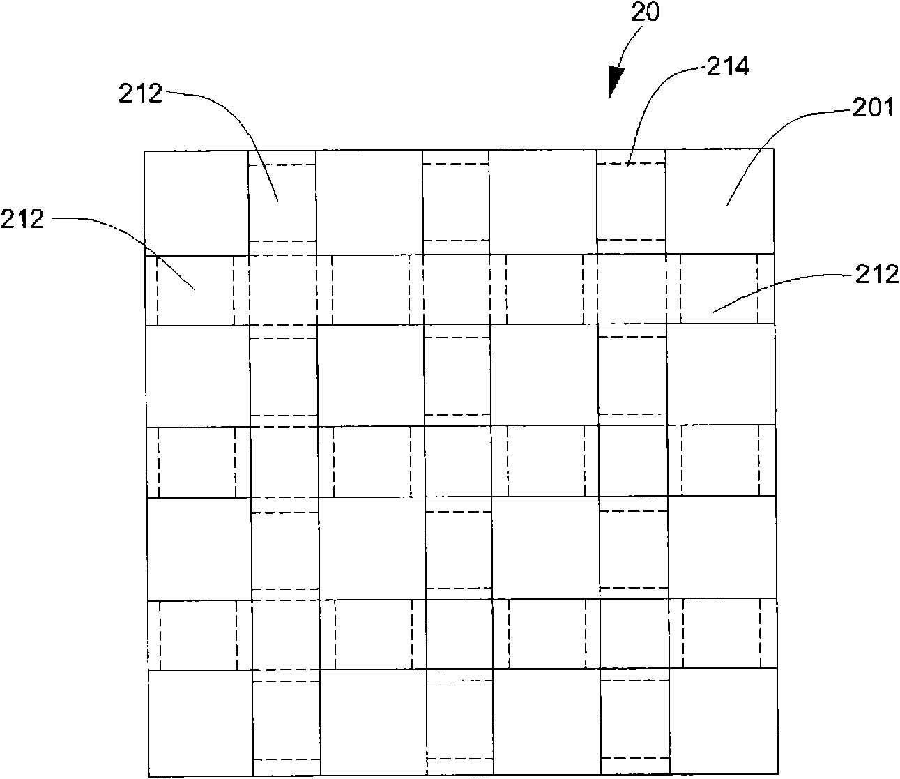
[0044] The direction of the present invention discussed here is a die reconfiguration packaging method, a method of reconfiguring a plurality of dies on a die holder and then packaging them. In order to provide a thorough understanding of the present invention, detailed steps and components thereof will be set forth in the following description. Obviously, the practice of the invention is not limited to the specific details of the manner in which wafers are stacked to which those skilled in the art are familiar. On the other hand, well-known wafer formation methods and detailed steps of back-end processes such as wafer thinning are not described in detail to avoid unnecessary limitations of the present invention. However, for the preferred embodiments of the present invention, it will be described in detail as follows, but in addition to these detailed descriptions, the present invention can also be widely implemented in other embodiments, and the scope of the present inventio...


PUM


Abstract

The invention relates to an encapsulation structure for modularization crystal grains, comprising a crystal grain accommodation bracket, an encapsulation body, a plurality of patterning first protection layers, a plurality of patterning metal line segments, a plurality of patterning second protection layers, a plurality of patterning UBM layers and a plurality of conductive elements, wherein the crystal grain accommodation bracket is provided with a plurality of crystal grain accommodation areas and a plurality of crystal grains, an active face of each crystal grain is provided with a plurality of welding disks, and the back face of each crystal grain is fixedly connected on the front faces of the crystal grain accommodation areas; the encapsulation body annually covers the crystal grain accommodation bracket with the plurality of crystal grains and the four faces of every crystal grain with the welding disks exposed; the patterning first protection layers covers the active faces of the crystal grains, with the welding disks exposed; one end of every patterning metal line segment is electrically connected with the welding disks, and the other end covers the surfaces of the first protection layers; the patterning second protection layers cover the metal line segments, parts of the surfaces of the fanning-out structures of the metal line segments are exposed, and the fanning-out structures are extended towards the exterior sides of the active faces of the crystal grains; the patterning UBM layers are formed on the surface of the fanning-out structure of every metal line segment, the fanning-out structure is extended towards the exterior side, and the patterning UBM layers are electrically connected with the metal line segments; and the conductive elements are electrically connected with the metal line segments by the UBM layers.

Description

technical field [0001] The present invention relates to a packaging method for crystal grain reconfiguration, in particular to a packaging method for crystal grain reconfiguration by using a crystal grain accommodation frame. Background technique [0002] Semiconductor technology has developed quite rapidly, so the miniaturized semiconductor die (Dice) must have diversified functional requirements, so that the semiconductor die must be configured with more input / output pads in a small area (I / O pads), thus making the density of metal pins (pins) also increase rapidly. Therefore, the early lead frame packaging technology is no longer suitable for high-density metal pins; therefore, a ball array (Ball Grid Array: BGA) packaging technology has been developed. The ball array package has the advantage of higher density than the lead frame package. In addition, its solder balls are less prone to damage and deformation. [0003] With the popularity of 3C products, such as: mobile...

Claims


Application Information

Patent Timeline
IPC IPC(8): H01L21/50H01L21/56H01L21/60H01L21/78H01L23/31H01L23/48
CPCH01L24/19H01L24/96H01L2224/73267H01L24/20H01L24/97H01L2224/0401H01L2224/04105H01L2224/12105H01L2224/19H01L2224/20H01L2224/92244H01L2224/97H01L2924/181H01L2924/3511
Inventor 沈更新
Owner CHIPMOS TECH INC
Learn More