Colored filter substrate, manufacture method thereof and liquid crystal display panel
A color filter technology and a manufacturing method, applied in optics, optomechanical equipment, nonlinear optics, etc., can solve the problems of poor PI climbing ability, no PI layer, light leakage, etc., to avoid embedded overlap , The effect of reducing the production cycle and reducing the production cost
- Summary
- Abstract
- Description
- Claims
- Application Information
AI Technical Summary
Problems solved by technology
Method used
Image

Examples
no. 1 example
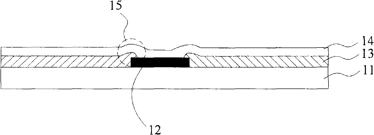
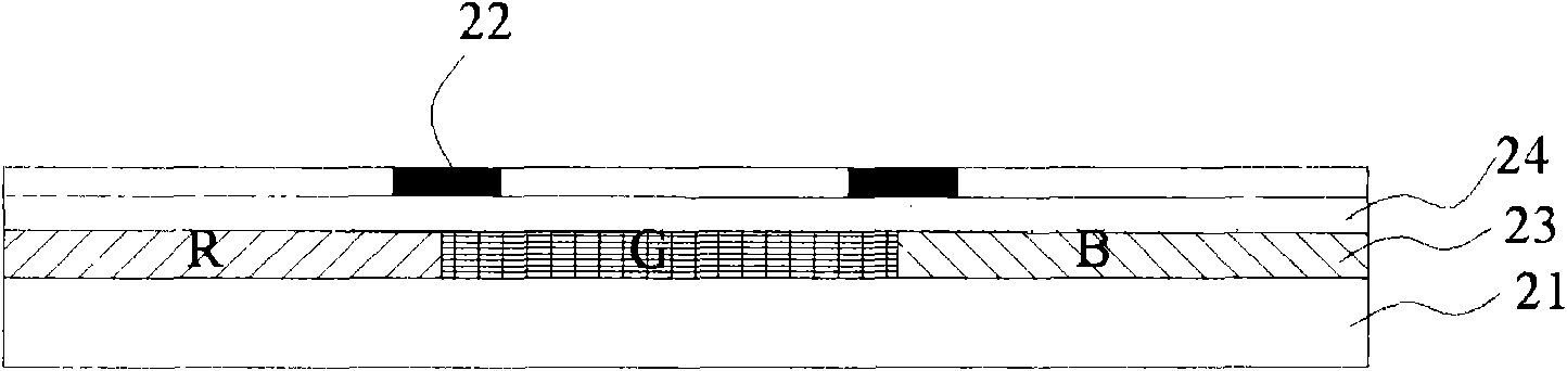
[0051] The sectional view of the color filter substrate of the first embodiment of the present invention is as follows figure 2 As shown, in this embodiment, the color filter substrate mainly includes: a substrate 21 , a black matrix layer 22 , a color resist layer 23 and a transparent conductive layer 24 . The substrate 21 is transparent, and may be a hard substrate made of glass, quartz, etc., or a flexible substrate made of plastic, polymer material, or the like. The color-resist layer 23 is directly formed on the substrate 21. Same as the prior art, the different areas of the color-resist layer 23 are respectively set as red (R), green (G), and blue (B) color-resist. The light is displayed as red, green and blue respectively, and the red (R), green (G), and blue (B) color resists are closely adjacent or there are gaps. The transparent conductive layer 24 is located on the color resist layer 23, and the material of the transparent conductive layer 24 is required to be a tra...
no. 2 example
[0066] The sectional view of the color filter substrate of the second embodiment of the present invention is as follows Figure 4 As shown, in this embodiment, the color filter substrate mainly includes: a substrate 41 , a black matrix layer 42 , a color resist layer 43 and a transparent conductive layer 44 . The materials selected for the components of the color filter substrate in this embodiment are the same as those in the first embodiment, and will not be repeated here. Compared with the first embodiment, the difference of the color filter substrate shown in the second embodiment is that the black matrix layer 42 is directly on the substrate 41, the color resist layer 43 is on the black matrix layer 42, and the transparent conductive layer 44 is on the on the color resist layer 43 .
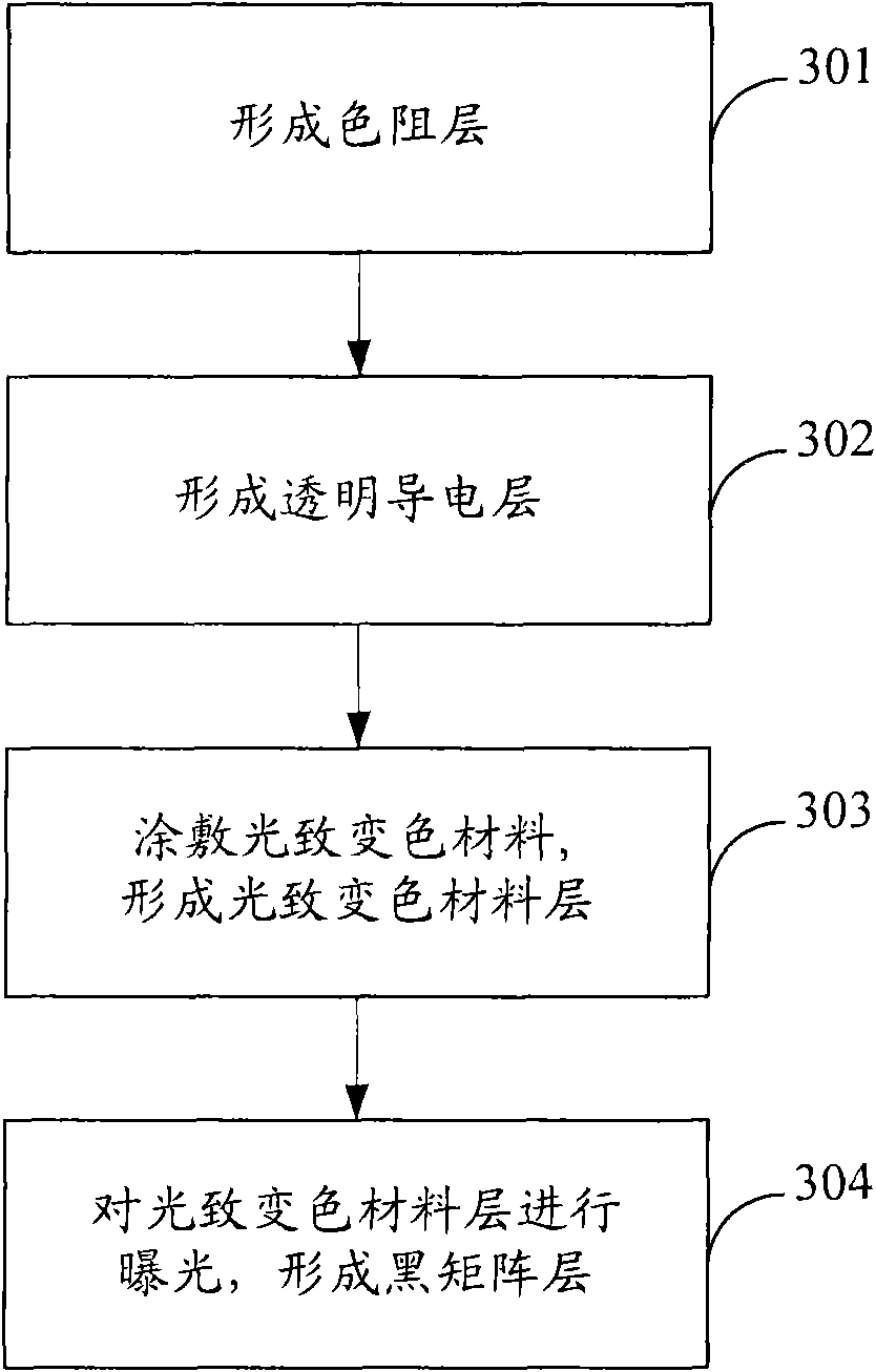
[0067] In this embodiment, the process flow of the manufacturing method of the color filter substrate is as follows Figure 5 As shown, it mainly includes the following steps:
[0068] St...
no. 3 example
[0077] The sectional view of the color filter substrate of the third embodiment of the present invention is as follows Figure 6 As shown, in this embodiment, the color filter substrate mainly includes: a substrate 61 , a black matrix layer 62 , a color resist layer 63 and a transparent conductive layer 64 . The materials selected for the components of the color filter substrate in this embodiment are the same as those in the first embodiment, and will not be repeated here. Compared with the first embodiment, the difference of the color filter substrate shown in the third embodiment is that the color resist layer 63 is located on the substrate 61, the black matrix layer 62 is located on the color resist layer 63, and the transparent conductive layer 64 is located on the black matrix layer 62.
[0078] In this embodiment, the process flow of the manufacturing method of the color filter substrate is as follows Figure 7 As shown, it mainly includes the following steps:
[007...
PUM
 Abstract
Description
Claims
Application Information
 - R&D
- Intellectual Property
- Life Sciences
- Materials
- Tech Scout
- Unparalleled Data Quality
- Higher Quality Content
- 60% Fewer Hallucinations
Browse by: Latest US Patents, China's latest patents, Technical Efficacy Thesaurus, Application Domain, Technology Topic, Popular Technical Reports.
© 2025 PatSnap. All rights reserved.Legal|Privacy policy|Modern Slavery Act Transparency Statement|Sitemap|About US| Contact US: help@patsnap.com