Supercharge Your Innovation With Domain-Expert AI Agents!

Dynamic random access memory and memory array

A dynamic random access and memory array technology, applied in the fields of semiconductor/solid-state device components, electric solid-state devices, semiconductor devices, etc., can solve the problem of miniaturization of chip size that cannot simultaneously shorten the access time of word lines, and achieve faster speed. The effect of access time

Active Publication Date: 2010-12-08
NAN YA TECH
View PDF6 Cites 0 Cited by
  • Summary
  • Abstract
  • Description
  • Claims
  • Application Information

AI Technical Summary

Problems solved by technology

Therefore, the requirements of shortening the access time of the word line and miniaturization of the chip size cannot be taken into account at the same time.

Method used


Image

  • Dynamic random access memory and memory array
  • Dynamic random access memory and memory array
  • Dynamic random access memory and memory array

Examples


Embodiment Construction

[0061] The present invention will be more fully described hereinafter with reference to the accompanying drawings, in which various embodiments of the invention are shown. This invention may, however, be embodied in many different forms and should not be construed as limited to the embodiments set forth herein. Rather, these embodiments are provided so that this disclosure will be thorough and complete, and will fully convey the scope of the invention to those skilled in the art. In the drawings, the size and relative sizes of layers and regions may be exaggerated for clarity.

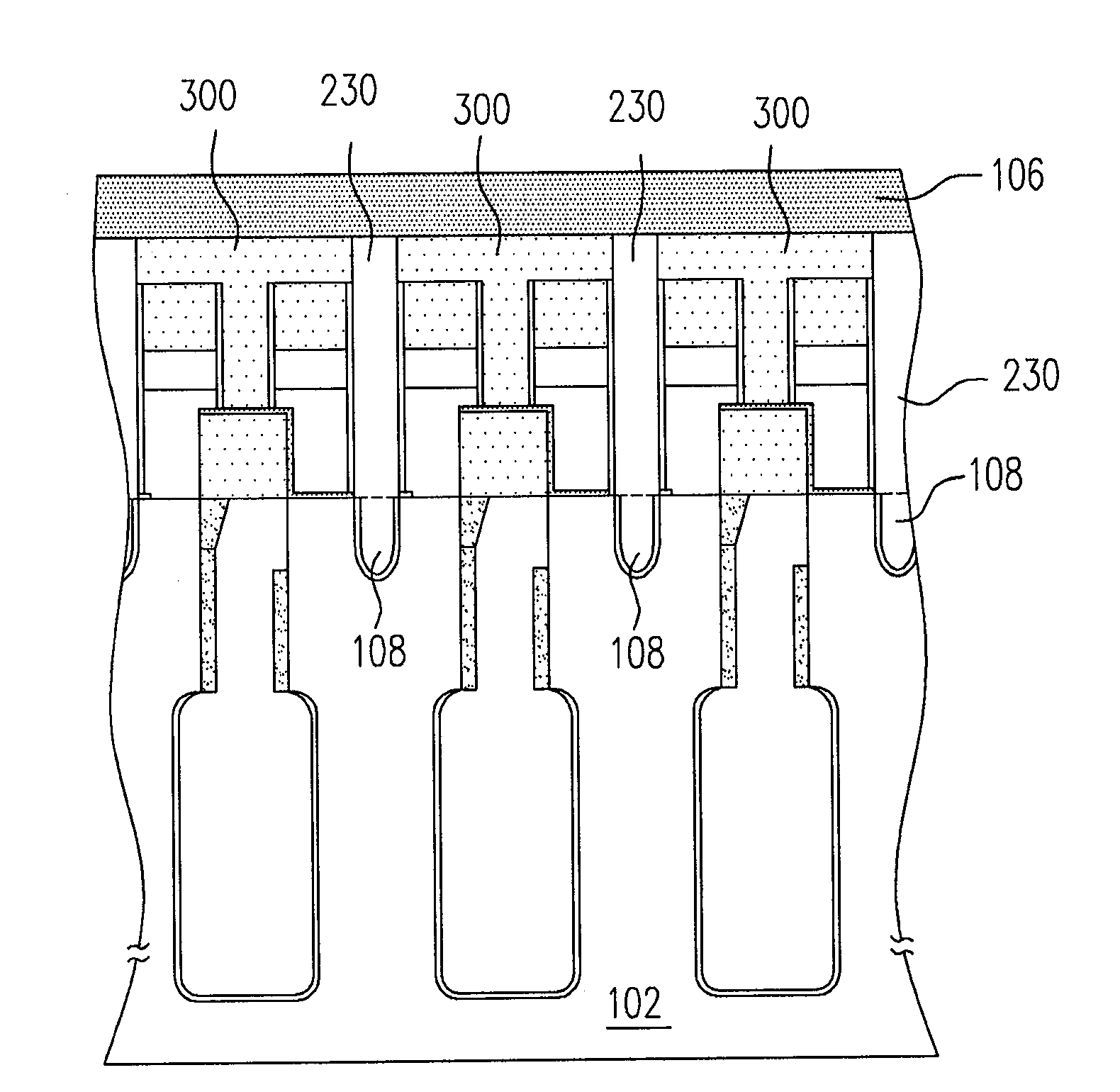
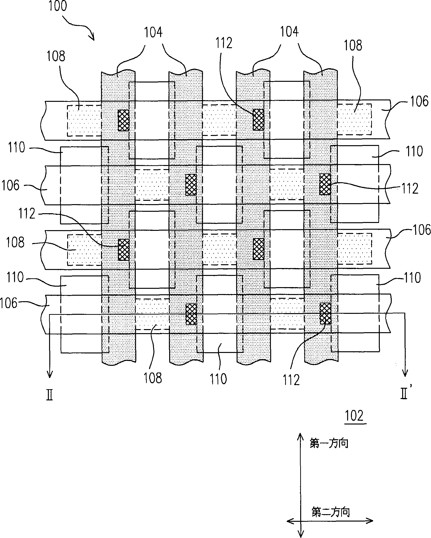
[0062] figure 1 It is a schematic top view of a dynamic random access memory according to the first embodiment of the present invention.

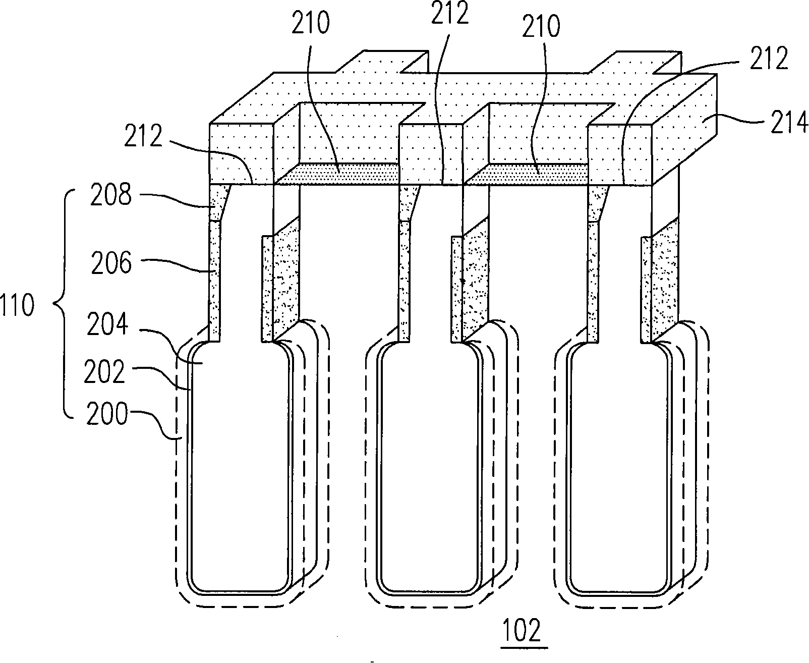
[0063] Please refer to figure 1 , the DRAM 100 of the first embodiment includes a substrate 102 , a bit line 104 , a word line 106 , a recessed channel 108 and a trench capacitor 110 . The bit lines 104 are arranged on the substrate 102 in a first direction, and...


PUM


Abstract

The invention discloses a dynamic random access memory comprising a substrate, bit lines, word lines, a concave channel, a conductive plunger and a trench type capacitor, wherein the bit lines are configured on the substrate in a first direction, and the word lines are configured on the bit lines in a second direction. The concave channel is positioned in the substrate between the two bit lines below the word lines, and the conductive plunger is connected with the concave channel and the bit lines. The trench type capacitor is configured in the substrate between the two bit lines outside the concave channel. The word lines can be electrically connected with the concave channel directly in the mode of without increasing a chip area, so the access time of the word lines can be accelerated without increasing the chip size.

Description

technical field [0001] The present invention relates to a memory structure, and in particular to a Dynamic Random Access Memory (DRAM) and a memory array. Background technique [0002] As far as the memory is concerned, in order to turn on the memory cells of the same word line without obvious delay time, the word line structure is often designed as a stitch or a segment structure. Such as the technology of US Patent No. 6,043,562 or 6,057,573. However, since the above-mentioned structures require additional space for setting the stitched word line contact window (WL contact) and the word line branch drive circuit (drive IC), the chip size is increased while reducing the delay time. Therefore, it is impossible to meet the requirements of shortening the access time of the word line and miniaturizing the chip size at the same time. Contents of the invention [0003] The invention provides a dynamic random access memory, which can speed up the access time of the word line w...

Claims


Application Information

Patent Timeline
Patent Type & Authority Patents(China)
IPC IPC(8): H01L27/108H01L23/522H10B12/00
Inventor 黄文魁
Owner NAN YA TECH
Features
  • R&D
  • Intellectual Property
  • Life Sciences
  • Materials
  • Tech Scout
  • Unparalleled Data Quality
  • Higher Quality Content
  • 60% Fewer Hallucinations
Learn More