Dye-sensitized optotransistor and preparation method thereof

A phototransistor and dye sensitization technology, applied in the fields of photosensitive equipment, semiconductor/solid-state device manufacturing, photovoltaic power generation, etc., can solve the problems of high cost and complicated etching method, and achieve the effect of low material cost

Active Publication Date: 2009-12-23
SHANGHAI UNIV
View PDF0 Cites 3 Cited by
  • Summary
  • Abstract
  • Description
  • Claims
  • Application Information

AI Technical Summary

Problems solved by technology

But these etching meth...

Method used


Image

  • Dye-sensitized optotransistor and preparation method thereof
  • Dye-sensitized optotransistor and preparation method thereof
  • Dye-sensitized optotransistor and preparation method thereof

Examples


Embodiment Construction

[0027] In order to describe the technical content, structural features, achieved goals and effects of the present invention in detail, the following will be described in detail in conjunction with examples and diagrams.

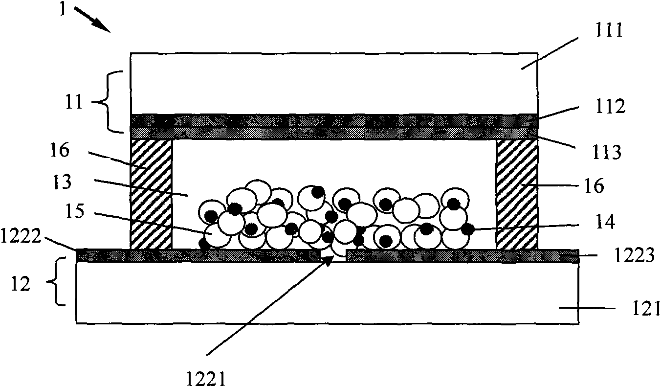
[0028] figure 1 A dye-sensitized phototransistor 1 based on a dye-sensitized cell structure is shown. The dye-sensitized phototransistor 1 includes a first electrode 11 and a second electrode 12 facing to each other, an electrolyte 13 between the first electrode 11 and the second electrode 12, a dye sensitizer 14, and an adhesive formed on the second electrode. Nanocrystalline semiconductor 15 on two electrodes 12 . The nanocrystalline semiconductor 15 is preferably titanium dioxide nanocrystalline particles. The first electrode 11 and the second electrode 12 are sealed together by a heat-sealing film 16 . The dye sensitizer 14 is adsorbed on the surface of the nanocrystalline semiconductor 15 . The first electrode 11 includes a first glass substrate 111 ...


PUM

PropertyMeasurementUnit
Groove widthaaaaaaaaaa

Abstract

The invention discloses a dye-sensitized optotransistor and a preparation method thereof. The dye-sensitized optotransistor comprises a first electrode and a second electrode, an electrolyte, a dye sensitizer and a nanocrystal semiconductor, the electrolyte and the dye sensitizer are arranged between the first electrode and the second electrode, and the nanocrystal semiconductor is formed on the second electrode in an adherence manner. The second electrode is composed of a transparent substrate and a conducting layer formed on the transparent substrate, the conducting layer is generated by segmentation of an insulating channel to form a source electrode and a drain electrodetwo at two sides of the insulating channel and the nanocrystal semiconductor covers the insulating channel, the source electrode and the drain electrode. A second conducting layer of the second electrode is segmented into a source electrode and a drain electrode by electroetching, thus obtaining the novel dye-sensitized optotransistor based on a dye-sensitized cell unit structure. The dye-sensitized optotransistor of the invention adopts an oxide wide band gap semiconductor, which has the advantages of low material cost, insensitivity to background noise and capability of enlarging spectral response range by selection of various dyes.

Description

technical field [0001] The invention relates to a transistor and a preparation method thereof, in particular to a dye-sensitized phototransistor and a preparation method thereof. Background technique [0002] Phototransistor is an important device in the field of optical fiber communication, which has the functions of photoelectric conversion, light control switch, light detector, and light control logic device. Due to the recombination mechanism of photogenerated electrons and holes in the material itself, even if there is light irradiation, it still cannot provide significant photogenerated current under the source-drain voltage. In order to overcome this difficulty, the usual practice is to add an insulating layer and a back gate electrode on the back of the device (non-irradiated side), and use the electrostatic Coulomb force of the external bias to attract a certain kind of carrier, so that the photogenerated electrons and holes Spatial separation is generated in the m...

Claims


Application Information

Patent Timeline
IPC IPC(8): H01L51/42H01L51/05H01L51/48H01L51/40H01L51/00H01G9/20
CPCY02E10/542Y02E10/549
Inventor 王晓祺蔡传兵刘志勇鲁玉明周文谦
Owner SHANGHAI UNIV
Why Eureka
Try Eureka