Coplanar waveguide structure applying microwave photonic crystal

A technology of microwave photonics and coplanar waveguides, which is applied in waveguides, waveguide-type devices, circuits, etc., can solve the problems of large crosstalk and leakage, and restrict the development of integrated circuits, and achieve the simplification of preparation process, reduction of signal leakage, and improvement of transmission coefficient. Effect

Inactive Publication Date: 2009-12-23
INST OF SEMICONDUCTORS - CHINESE ACAD OF SCI
View PDF0 Cites 9 Cited by
  • Summary
  • Abstract
  • Description
  • Claims
  • Application Information

AI Technical Summary

Problems solved by technology

[0002] The design of integrated circuits is developing in the direction of high frequency, small size, and multiple components, which leads to increasing crosstalk and leakage between components and transmission lines inside the circuit, especially when the signal line turns, which seriously restricts development of integrated circuits

Method used


Image

  • Coplanar waveguide structure applying microwave photonic crystal
  • Coplanar waveguide structure applying microwave photonic crystal

Examples


Embodiment Construction

[0027] In order to make the object, technical solution and advantages of the present invention clearer, the present invention will be described in further detail below in conjunction with specific embodiments and with reference to the accompanying drawings.

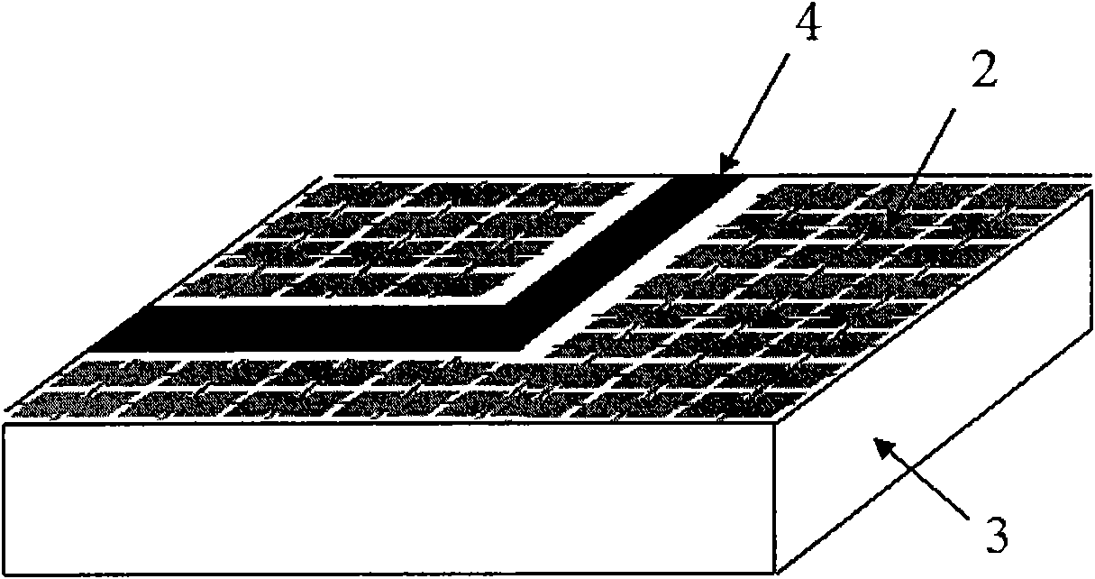
[0028] see figure 1 with figure 2 , figure 1 It is a perspective view of a coplanar waveguide structure using a microwave photonic crystal provided by the present invention, and the structure includes a dielectric layer 3 , a photonic crystal ground plane 2 and a central conductor 4 . Among them, the dielectric layer 3 is used for high-frequency transmission. The photonic crystal ground plane 2 is used to confine electromagnetic waves. The photonic crystal ground plane 2 is located on the dielectric layer 3 and closely combined with the dielectric layer 3 . The central conductor 4 is used to transmit electromagnetic waves. The central conductor 4 is an L-shaped matching copper wire, which is bent at 90 degrees in the ...


PUM

PropertyMeasurementUnit
Thicknessaaaaaaaaaa
Thicknessaaaaaaaaaa
Resistanceaaaaaaaaaa

Abstract

The invention discloses a coplanar waveguide structure applying microwave photonic crystal. The structure comprises a dielectric layer (3) for high-frequency transmission, a photonic crystal ground plane (2) for limiting electromagnetic wave and a central conductor (4) for transmitting the electromagnetic wave, wherein the photonic crystal ground plane (2) is formed by connecting a plurality of microwave photonic crystal unit structures (1), is positioned above the dielectric layer (3) and is tightly combined with the dielectric layer (3); the central conductor (1) is an L-type 50 ohm copper conducting wire; the middle position of the conducting wire is bent for 90 degrees; and the central conductor (4) is positioned above the dielectric layer (3) and tightly combined with the dielectric layer (3). The provided coplanar waveguide structure applying the microwave photonic crystal effectively reduces the signal leakage, simplifies a preparation process to enable the process to be more suitable for monolithic microwave integration, and can improve the transmission coefficient of the real-coplanar waveguide.

Description

technical field [0001] The present invention relates to the technical field of microwave circuit preparation, and more specifically, relates to a coplanar waveguide structure using microwave photonic crystals, which can effectively reduce signal leakage and loss caused by the ninety-degree turn of the microstrip line. The problem of signal incompleteness can be solved, and the transmission coefficient of the coplanar waveguide in the embodiment can be improved. Background technique [0002] The design of integrated circuits is developing in the direction of high frequency, small size, and multiple components, which leads to increasing crosstalk and leakage between components and transmission lines inside the circuit, especially when the signal line turns, which seriously restricts development of integrated circuits. Correspondingly, how to reduce the negative impact of this phenomenon is also a practical task faced by circuit design and application. [0003] Photonic cryst...

Claims


Application Information

Patent Timeline
IPC IPC(8): H01P3/08H01P3/00
Inventor 张昀哈森其其格任民鞠昱陈伟谢亮祝宁华
Owner INST OF SEMICONDUCTORS - CHINESE ACAD OF SCI
Why Eureka
Try Eureka