Luminescent device and manufacturing method thereof

A technology of light-emitting devices and light-emitting layers, which is applied in semiconductor/solid-state device manufacturing, semiconductor devices, electrical components, etc., can solve problems such as damage to the light-emitting performance of the LED structure 100, and overcome thermal expansion and lattice mismatch. The effect of throughput

Inactive Publication Date: 2009-12-30
潘晓和
View PDF0 Cites 9 Cited by
  • Summary
  • Abstract
  • Description
  • Claims
  • Application Information

AI Technical Summary

Problems solved by technology

As a result, the light emitting performance of the LED structure 100 may be impaired

Method used


Image

  • Luminescent device and manufacturing method thereof
  • Luminescent device and manufacturing method thereof
  • Luminescent device and manufacturing method thereof

Examples


Embodiment Construction

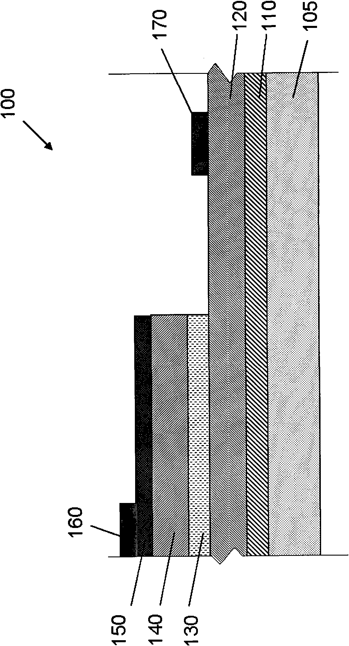
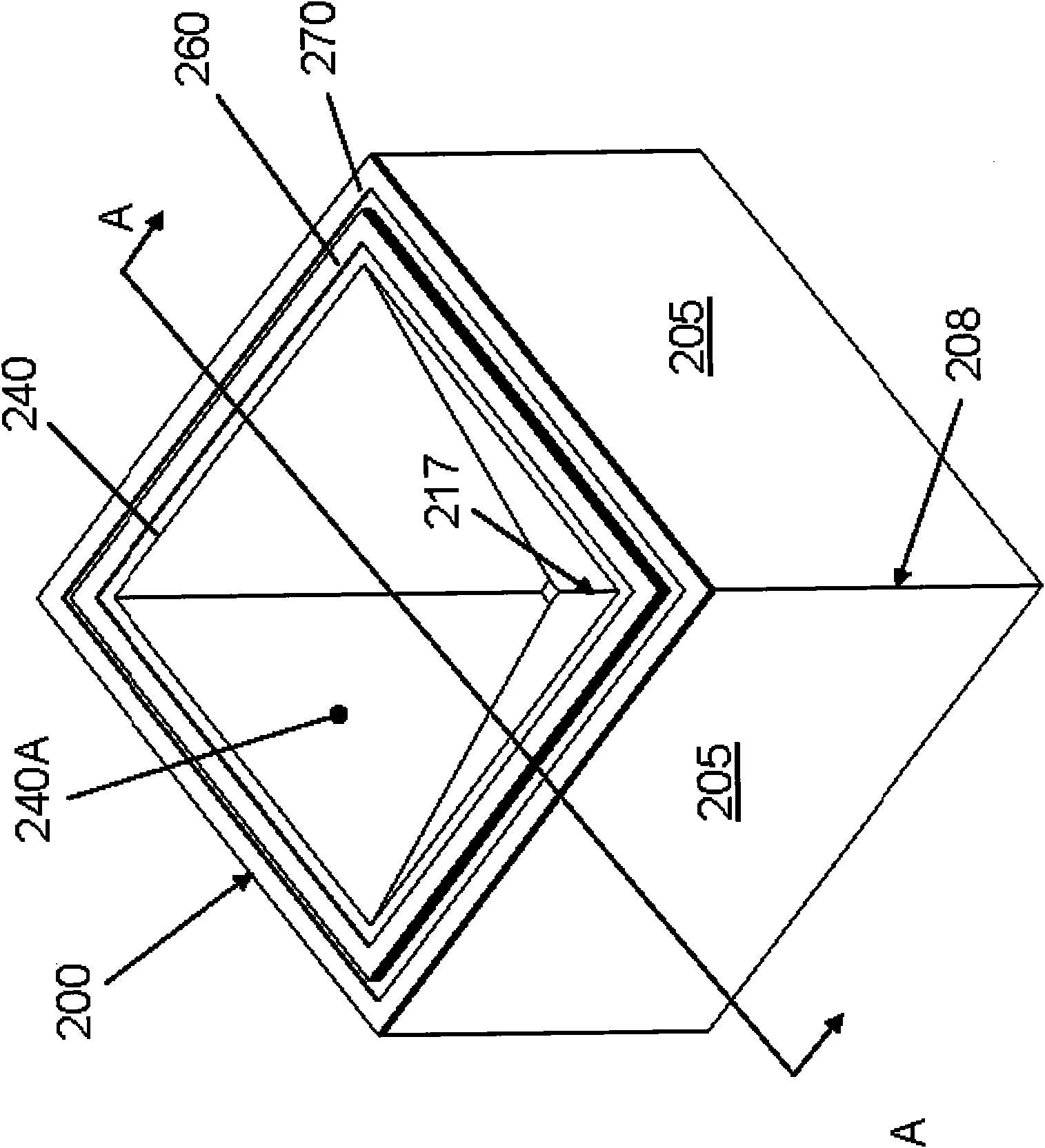
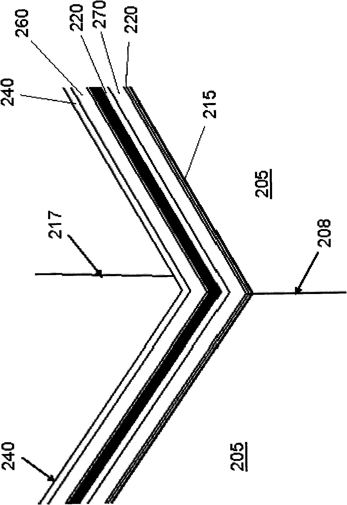
[0048] refer to Figure 2A to Figure 3C , having an upper surface 207 ( Figure 3B ) The light emitting device 200 is formed on the substrate 205. The light emitting device 200 includes a trench 210 in the substrate 205 below the upper surface 207 . The trench 210 has one or more trench surfaces 213 ( Figure 3B ). Trench 210 may also have a bottom surface 219 parallel to upper surface 207 . The area of ​​the bottom surface 219 can be kept less than 20% of one of the trench surfaces 213 . The substrate 205 may be silicon-based: the upper surface 207 may be parallel to the (100) crystal plane. The groove surface 213 may be parallel to the (111) crystal plane. (Alternatively, the upper surface 207 may be parallel to the (111) crystal plane. The trench surface 213 may be parallel to the (100) crystal plane.) The trench 210 may thus have the shape of an inverted pyramid or a truncated inverted pyramid in the substrate 205 shape, thereby forming a square opening in the upper...


PUM

PropertyMeasurementUnit
thicknessaaaaaaaaaa
thicknessaaaaaaaaaa
thicknessaaaaaaaaaa

Abstract

The present invention relates to a luminescent device and manufacturing method thereof. The luminescent device comprise a substrate having a first surface and a second surface not parallel to the first surface; and a luminescent layer arranged on the second surface to illumine. The luminescent layer has a luminescent surface not parallel to the first surface.

Description

technical field [0001] This patent application relates to a light emitting device. Background technique [0002] Solid-state light sources such as light-emitting diodes (LEDs) and solid-state lasers offer significant advantages over other forms of lighting such as incandescent or fluorescent lighting. For example, when LEDs or solid-state lasers are arranged as an array of red, green and blue elements, they can be used as a white light source or as a multicolor display. In such configurations, solid-state light sources are typically more efficient and generate less heat than traditional incandescent or fluorescent lights. Although solid-state lighting offers certain advantages, conventional semiconductor structures and devices for solid-state lighting are relatively expensive. One of the costs associated with conventional solid state light emitting devices relates to the relatively low manufacturing throughput of conventional solid state light emitting devices. [0003] r...

Claims


Application Information

Patent Timeline
Patent Type & Authority Applications(China)
IPC IPC(8): H01L33/00H01L33/12H01L33/16
CPCH01L21/02439H01L21/0243H01L21/02502H01L21/02433H01L33/12H01L33/16H01L33/007H01L21/02381H01L21/0237H01L21/0254
Inventor 潘晓和
Owner 潘晓和
Why Eureka
Try Eureka