Method for etching dielectric storage layer in flash memory
An electrical storage and storage layer technology, applied in the manufacture of circuits, electrical components, semiconductor/solid-state devices, etc., can solve the problems of corrosion, prolong the time of dry etching, affect the continuation of the process, etc., and achieve the effect of reducing damage
- Summary
- Abstract
- Description
- Claims
- Application Information
AI Technical Summary
Problems solved by technology
Method used
Image

Examples
Embodiment Construction
[0032] The specific implementation of the method for etching the dielectric storage layer in the flash memory provided by the present invention will be described in detail below in conjunction with the accompanying drawings.
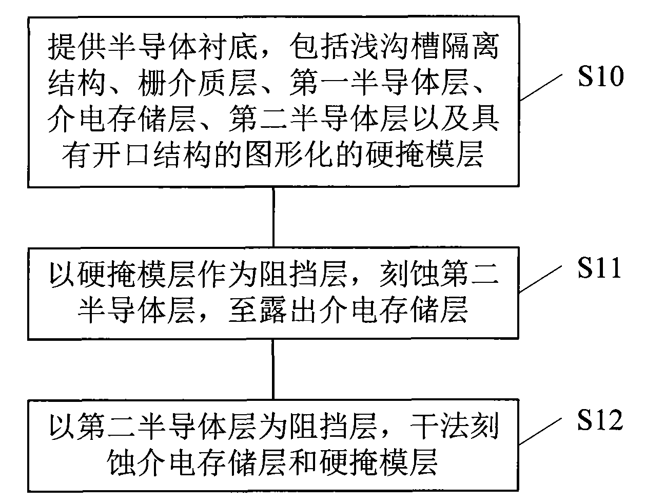
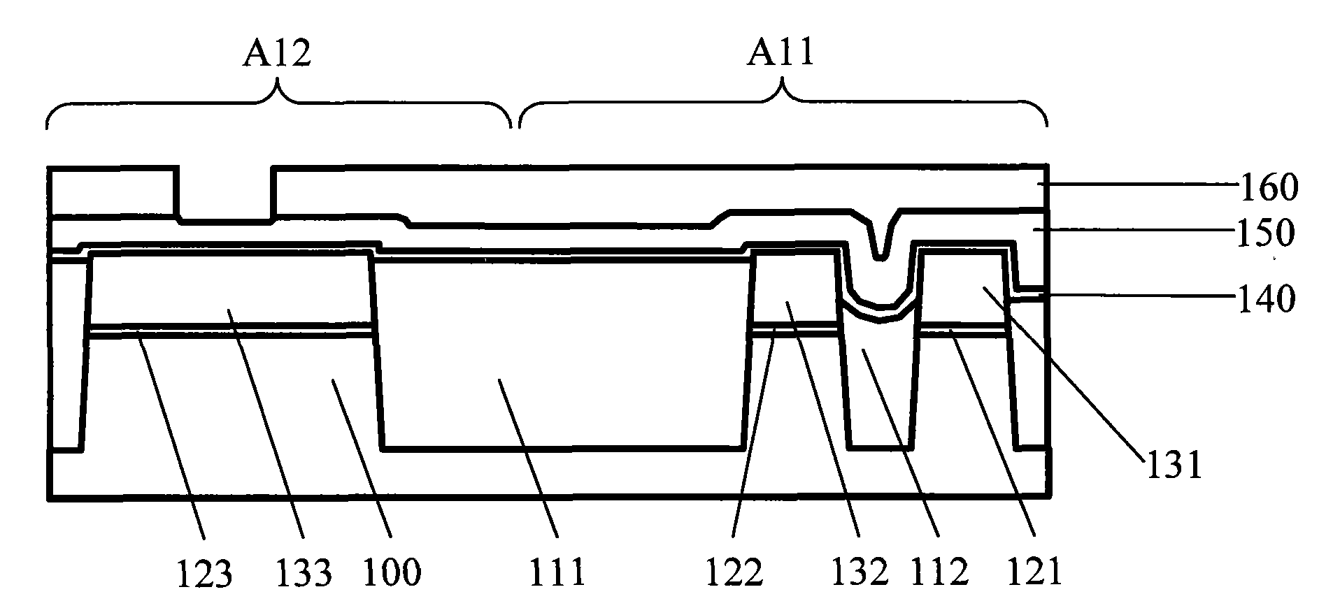
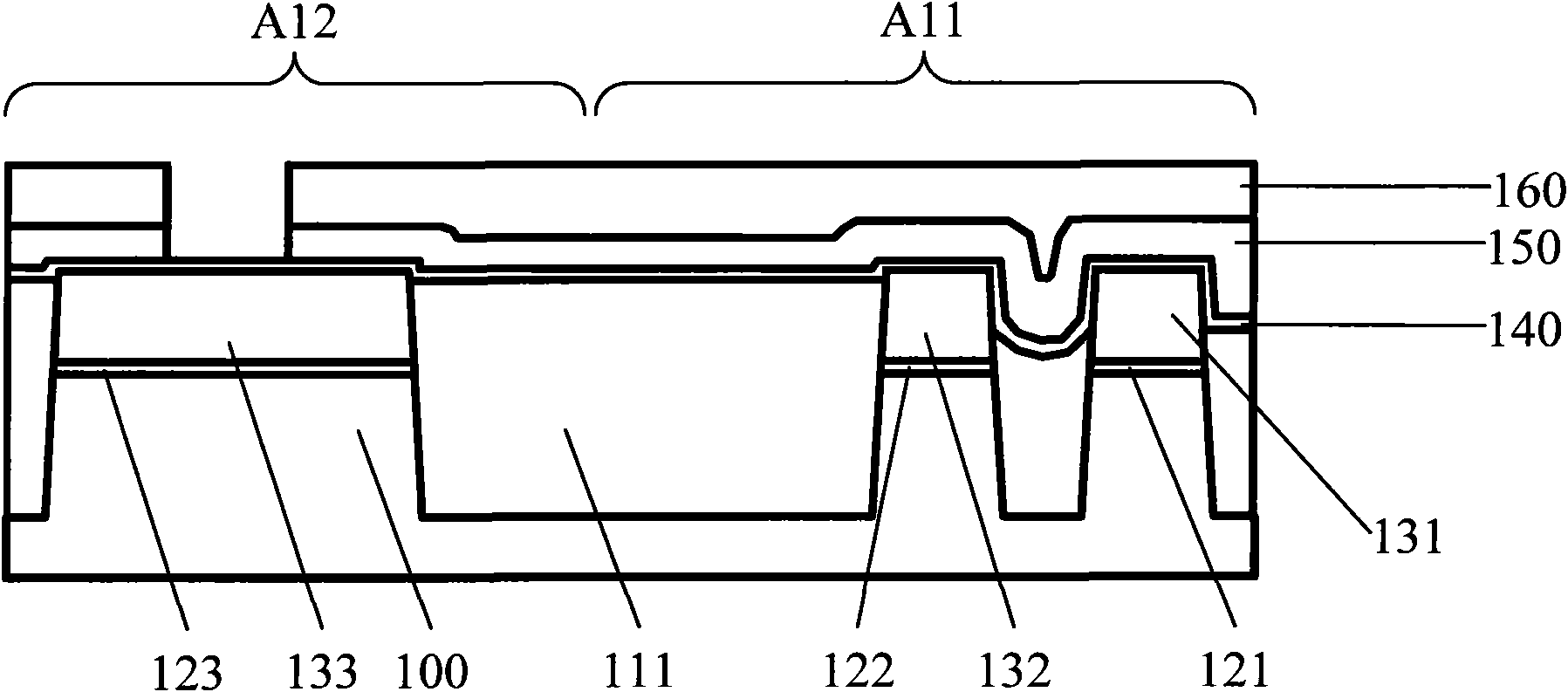
[0033] attached Image 6 Shown is a process flow chart of a specific embodiment of the method for etching a dielectric storage layer in a flash memory provided by the present invention. The method includes the following steps: Step S20, providing a semiconductor substrate, a gate dielectric layer, a first semiconductor layer located on the semiconductor substrate in sequence, a shallow trench located in the gate dielectric layer, the first semiconductor layer and the semiconductor substrate; A semiconductor layer and a shallow trench, a continuous dielectric storage layer away from the surface of the semiconductor substrate, a second semiconductor layer, and a hard mask layer with an opening structure; step S21, using the hard mask layer as a barrier lay...
PUM
 Abstract
Description
Claims
Application Information
 - R&D
- Intellectual Property
- Life Sciences
- Materials
- Tech Scout
- Unparalleled Data Quality
- Higher Quality Content
- 60% Fewer Hallucinations
Browse by: Latest US Patents, China's latest patents, Technical Efficacy Thesaurus, Application Domain, Technology Topic, Popular Technical Reports.
© 2025 PatSnap. All rights reserved.Legal|Privacy policy|Modern Slavery Act Transparency Statement|Sitemap|About US| Contact US: help@patsnap.com