Effective electrostatic discharge protection circuit

A technology for electrostatic discharge protection and protection circuits, applied in the field of ESD protection circuits, can solve problems such as uncontrollable reverse breakdown voltage, unsafe working mode, and chip failure, so as to improve ESD protection capabilities, competitiveness, and reliability. performance effect

Active Publication Date: 2010-01-06
WUXI CRYSTAL SOURCE MICROELECTRONICS CO LTD
View PDF0 Cites 5 Cited by
  • Summary
  • Abstract
  • Description
  • Claims
  • Application Information

AI Technical Summary

Problems solved by technology

The protection circuit formed by the diode has a simple structure and occupies almost no area (a diode can be formed through a parasitic PN junction). Its disadvantage is that the parameters of the diode are limited by the process parameters, the reverse breakdown voltage cannot be controlled and when the power supply When the forward pulse of ESD relative to ground is applied to VDD, the reverse breakdown of the diode is in an unsafe working mode, and thermal breakdown is prone to occur, resulting in short circuit or open circuit of the diode and causing chip failure.

Method used


Image

  • Effective electrostatic discharge protection circuit
  • Effective electrostatic discharge protection circuit
  • Effective electrostatic discharge protection circuit

Examples


Embodiment Construction

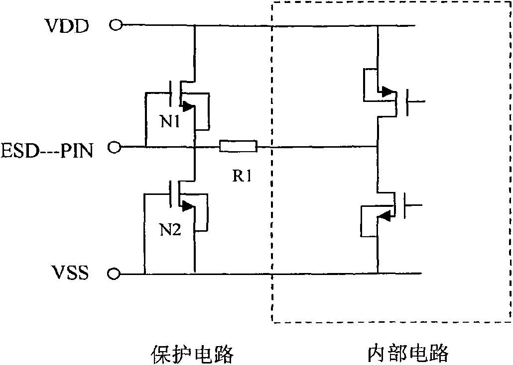
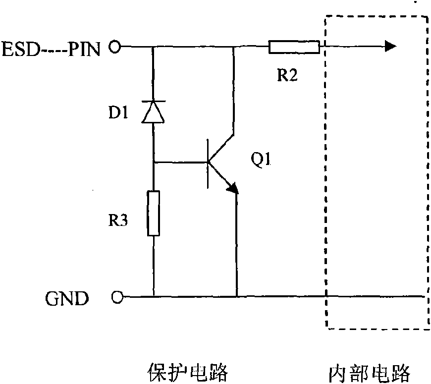
[0037] The effective ESD protection circuit of the present invention is divided into a protection circuit of a CMOS part and a protection circuit of a bipolar part; when being used for a CMOS protection circuit, the first NMOS transistor N1 and the second NMOS transistor N2 are connected in series, that is: the first The source of the NMOS transistor N1 is connected to the first power supply VDD, the drain of the first NMOS transistor N1 is connected to the source of the second NMOS transistor N2, the drain of the second NMOS transistor N2 is connected to the second power supply VSS; the drain of the first NMOS transistor N1 is connected to the second power supply VSS; The gate is connected to the pin of the CMOS part of the integrated circuit to be protected, that is, the electrostatic input terminal ESD---PIN (such as the pin of the CMOS part of the radio circuit, audio power amplifier circuit, such as audio input, output, etc.) and through the current limiting resistor R1 is...


PUM


Abstract

The invention relates to an effective electrostatic discharge protection circuit; electrostatic discharge (ESD) is the most important reliability problem in the current integrated circuits. Along with the development of manufacturing technology of the integrated circuits, characteristic dimension is reduced continuously, the anti-static electricity capacity is weaker, however, under the micro-electronic manufacturing and using environment, the chance that devices suffer from ESD is more, and the effect of the ESD on the integrated circuits is greater, and ESD damage is an attention focus on the new process. The invention starts from the basic starting point, the limit of the traditional simple ESD protective circuit is broken through, and the ESD protective circuit is improved on the structure with the consideration of domain layout and design rules, but the process flows are basically consistent with the regular BICMOS processes, thereby ensuring good ESD protecting capacity of the integrated circuits and being capable of not leading the process to be complicated, improving the reliability of the circuit without increasing cost and improving the competitiveness of the circuit.

Description

technical field [0001] The invention relates to an ESD protection circuit for providing effective ESD electrostatic protection inside an integrated circuit, and belongs to the technical field of semiconductor manufacturing. Background technique [0002] Electrostatic Discharge (ESD) is one of the most important reliability issues in today's integrated circuits. With the development of integrated circuit manufacturing technology, the feature size is continuously shrinking, and the antistatic ability is getting weaker and weaker. However, in the environment of microelectronics manufacturing and use, there are more and more opportunities for devices to suffer from ESD, which makes ESD harmful to the environment. The influence of integrated circuits is also increasing, and ESD damage has become the focus of attention in new processes. [0003] The ESD phenomenon can mainly cause the following damage to electronic devices: in semiconductor devices, the oxide film is ruptured due...

Claims


Application Information

Patent Timeline
Patent Type & Authority Applications(China)
IPC IPC(8): H02H9/00
Inventor 朱伟民马晓辉聂卫东陈东勤
Owner WUXI CRYSTAL SOURCE MICROELECTRONICS CO LTD
Why Eureka
Try Eureka