

Binding manufacture technology for electrical element of flat-panel display
A technology of flat panel display and electrical components, applied in the field of binding production technology of flat panel display electrical components
- Summary
- Abstract
- Description
- Claims
- Application Information
AI Technical Summary
Problems solved by technology
Method used
Image

Examples
Embodiment Construction
[0010] Now set forth the present invention in detail in conjunction with accompanying drawing:
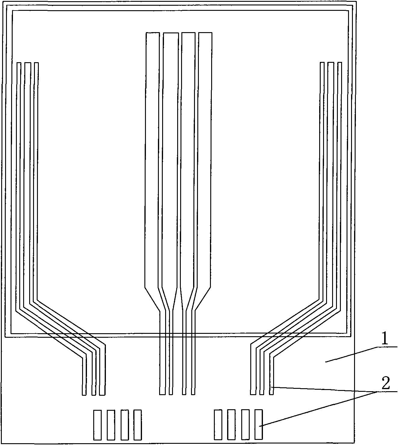
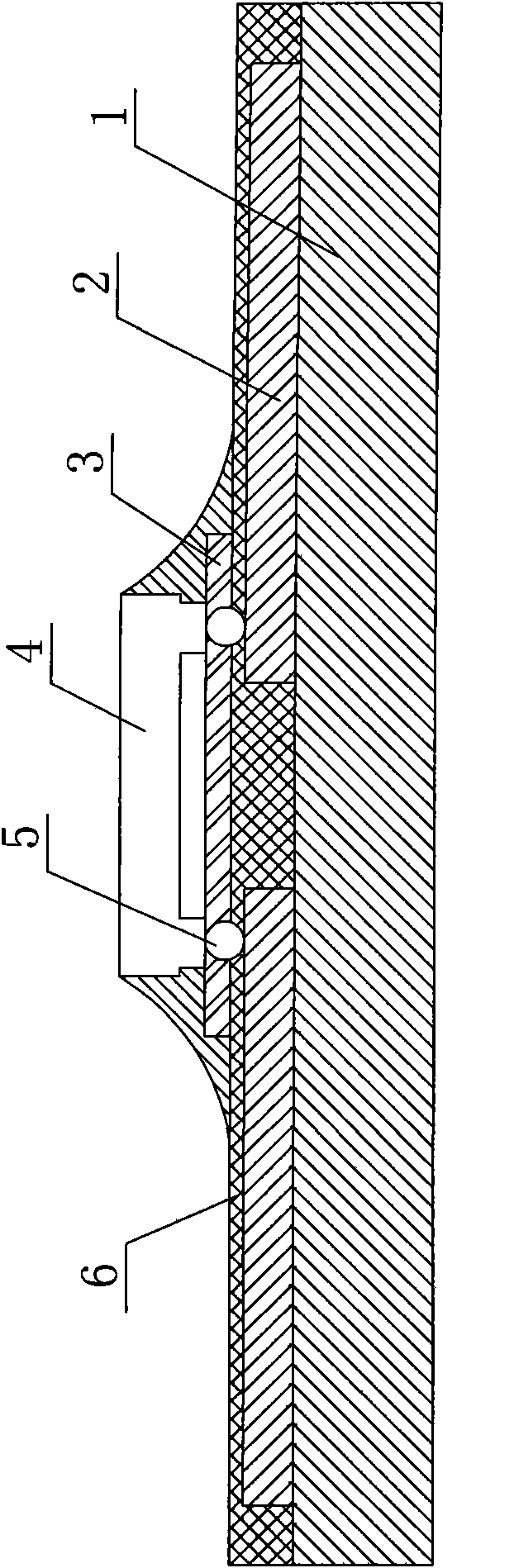
[0011] The present embodiment is to bind IC on the flat panel display substrate, and its process steps are: 1) make lead wire on the flat panel display substrate, carry out glass cutting process to lead wire; 2) clean lead wire; 3) coat protective film material on lead wire and pre-curing; 4) exposure treatment of the protective film; 5) development and main curing of the protective film to form the pattern required for the protective film; 6) paving the opposite sex conductive film and IC; 7) thermocompression bonding of the electrical components .
[0012] figure 1 with figure 2 Among them, 1 is the substrate, 2 is the lead wire, 3 is the anisotropic conductive film, 4 is the IC, 5 is the conductive ball, and 6 is the protective film.
[0013] The protective film material is thermoplastic resin or thermoplastic polymer containing polyamide. The characteristics of these two ma...
PUM
 Abstract
Description
Claims
Application Information