Supercharge Your Innovation With Domain-Expert AI Agents!

GaN-based multi-band detector and preparation method thereof

A gallium nitride-based and fabrication method technology, applied in semiconductor/solid-state device manufacturing, radiation control devices, electrical components, etc., can solve the problem of inability to distinguish and detect multiple discrete wavebands, which affects the development of gallium nitride ultraviolet detectors and Application and other issues

Inactive Publication Date: 2011-06-01
INST OF SEMICONDUCTORS - CHINESE ACAD OF SCI
View PDF0 Cites 0 Cited by
  • Summary
  • Abstract
  • Description
  • Claims
  • Application Information

AI Technical Summary

Problems solved by technology

But these detectors respond to light less than a certain wavelength, and cannot distinguish and detect multiple discrete wavelength bands
Influenced the further development and application of gallium nitride ultraviolet detectors

Method used


Image

  • GaN-based multi-band detector and preparation method thereof
  • GaN-based multi-band detector and preparation method thereof
  • GaN-based multi-band detector and preparation method thereof

Examples


Embodiment Construction

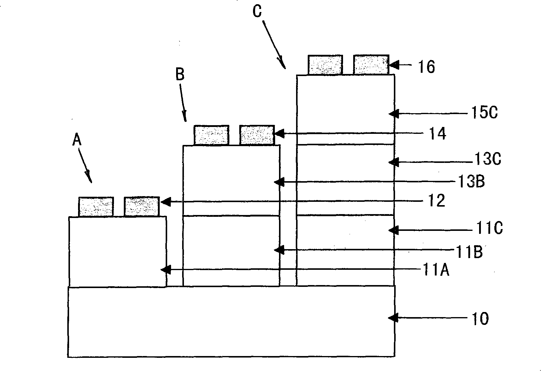
[0043] see figure 1 , figure 2 , image 3 As shown, a GaN-based multi-band detector of the present invention comprises:

[0044] A substrate 10, because the light needs to be incident from the back when the detector works, so the substrate material is double-sided polished sapphire;

[0045] The three-stage first, second, and third wide bandgap material layers 11A, 11B, and 11C are epitaxially grown on the substrate 10 at the same time. The first wide bandgap material layer 11A is used to detect light in a shorter wavelength band. According to the needs of the detection band and the continuous adjustability of the band gap of gallium nitride-based materials (including AlN, GaN, InN and their ternary or multi-component compounds), the material can be designed and selected so that the band gap width meets the needs of the detection band. For example, if it is necessary to detect light in the blind sunlight band, the first wide bandgap material layer 11A can be made of AlGaN...


PUM


Abstract

The invention discloses a GaN-based multi-band detector, which comprises a substrate, a short wave band detecting unit, a medium wave band detecting unit and a long wave band detecting unit, wherein the short wave band detecting unit comprises a first wide band gap material layer grown at one third part of one side of the upside of the substrate, and a pair of first back-to-back Schottky electrodes grown on the first wide band gap material layer; the medium wave band detecting unit comprises a second wide band gap material layer grown at one third part of the middle of the upside of the substrate, a second middle band gap material layer grown on the second wide band gap material layer, and a pair of second back-to-back Schottky electrodes grown on the second middle band gap material layer; and the long wave band detecting unit comprises a third wide band gap material layer grown at one third part of the other side of the upside of the substrate, a third middle band gap material layer grown on the third wide band gap material layer, a third narrow band gap material layer grown on the third middle band gap material layer, and a pair of third back-to-back Schottky electrodes grown onthe third narrow band gap material layer.

Description

technical field [0001] The invention belongs to the field of semiconductor devices, in particular a gallium nitride-based multi-band detector and a manufacturing method thereof. Background technique [0002] As a third-generation semiconductor, gallium nitride (GaN) and its series of materials (including aluminum nitride, aluminum gallium nitride, indium gallium nitride, and indium nitride) are characterized by their large band gap and wide spectral range (covering from ultraviolet to Infrared full band), high temperature resistance and corrosion resistance, it has great application value in the field of optoelectronics and microelectronics. GaN-based ultraviolet detector is a very important GaN-based optoelectronic device, which is widely used in civil and military fields such as missile early warning, rocket plume detection, ultraviolet communication, biochemical weapon detection, aircraft guidance, spacecraft, ozone layer hole detection, fire monitoring, etc. important a...

Claims


Application Information

Patent Timeline
Patent Type & Authority Patents(China)
IPC IPC(8): H01L27/144H01L21/84
Inventor 刘文宝孙苋赵德刚刘宗顺张书明朱建军杨辉
Owner INST OF SEMICONDUCTORS - CHINESE ACAD OF SCI
Features
  • R&D
  • Intellectual Property
  • Life Sciences
  • Materials
  • Tech Scout
  • Unparalleled Data Quality
  • Higher Quality Content
  • 60% Fewer Hallucinations
Learn More