Novel C-band microstrip antenna with negative permeability material
A negative magnetic permeability material, the technology of microstrip antenna, applied in the direction of antenna, antenna array, radiating element structure, etc., can solve the problems of low gain, narrow operating frequency band of microstrip antenna, and large influence on antenna performance, so as to improve the gain. , the effect of improving the signal receiving ability and transmitting ability
- Summary
- Abstract
- Description
- Claims
- Application Information
AI Technical Summary
Problems solved by technology
Method used
Image

Examples
Embodiment 1
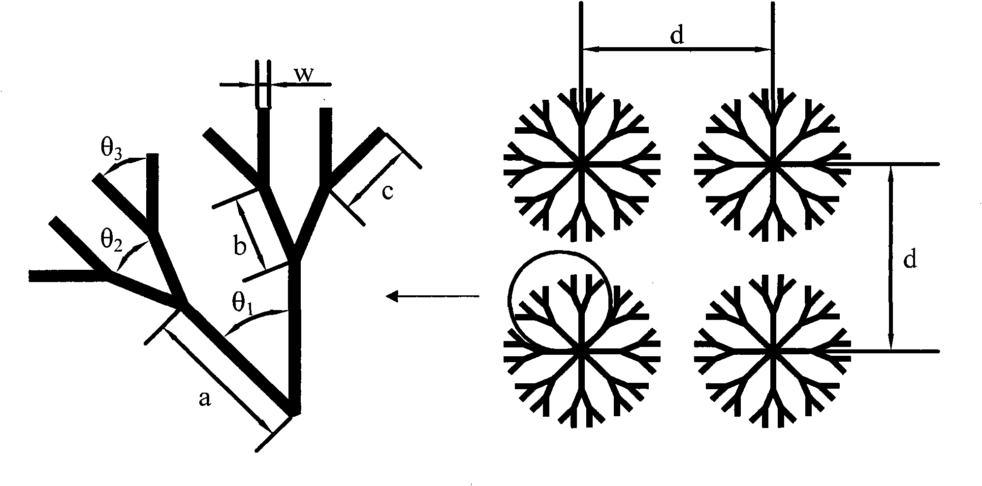
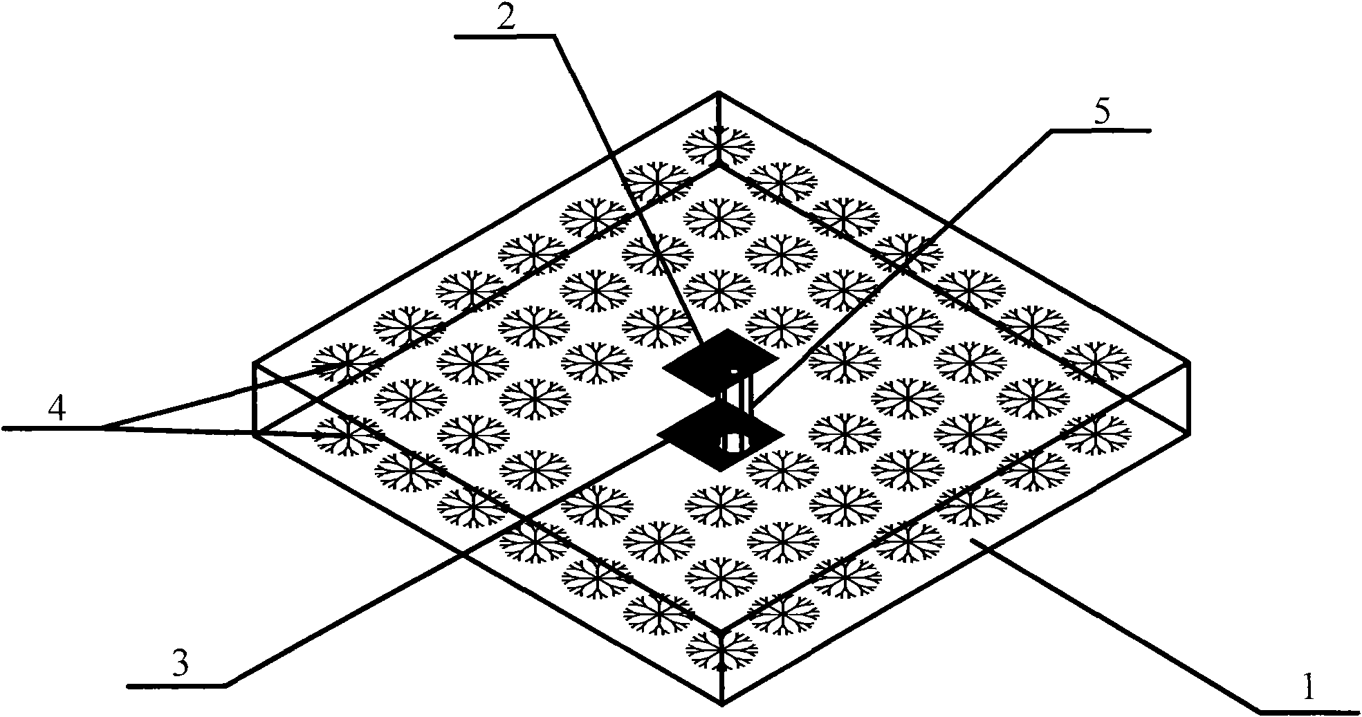
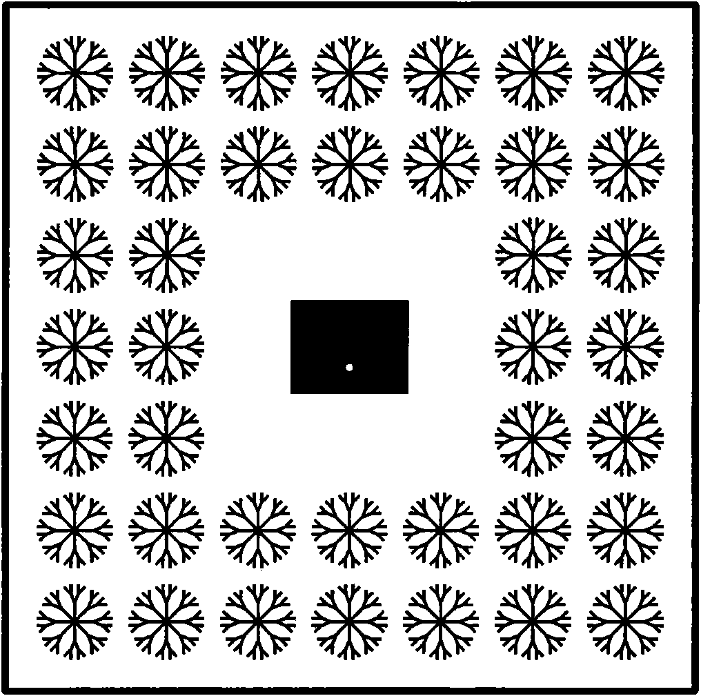
[0017] Using circuit board etching technology to produce a microstrip antenna with a double-sided dendritic structure with a central operating frequency of 5.28GHz, such as figure 2 shown. image 3 and Figure 4 The front and rear views of the antenna are shown respectively. A polytetrafluoroethylene material (ε=2.65) with an area of 120mm×120mm and a thickness of 1.5mm is selected as the dielectric substrate 1 of the antenna, and the size of the metal copper radiation patch 2 on one side of the dielectric substrate is 20.6mm×16.3mm. The metal grounding plate 3 is etched on one side, and the grounding plate is slightly larger than the radiation patch, measuring 30mm×30mm. The dendritic structure 4 is etched on both sides in the blank space around the radiation patch and the ground plane, and the dendritic structures on both sides are strictly aligned. For the microstrip antenna of this embodiment, the geometric dimensions of the dendritic structure are: the length of the...
Embodiment 2
[0019] Similar to Example 1, use circuit board etching technology to manufacture a microstrip antenna with a double-sided dendritic structure at a center operating frequency of 6.53 GHz, and select a polytetrafluoroethylene material with an area of 90 mm × 90 mm and a thickness of 1 mm (ε=2.65) As the dielectric substrate of the antenna, the size of the metal copper radiation patch on one side of the dielectric substrate is 16.8mm×12.9mm, and the metal ground plate is etched on the other side, and the ground plate is slightly larger than the radiation patch, which is 25mm× 25mm. The dendritic structure is etched on both sides in the blank space between the radiation patch and the ground plane, and the dendritic structures on both sides are strictly aligned. For the microstrip antenna of this embodiment, the geometric dimensions of the dendritic structure are: the length of the first-level branch a=2.7mm, the length of the second-level branch b=1.3mm, the length of the third-...
Embodiment 3
[0021] Similar to Example 1, use circuit board etching technology to manufacture a microstrip antenna with a double-sided dendritic structure at a center operating frequency of 7.12 GHz, and use an epoxy glass cloth material with an area of 85 mm × 85 mm and a thickness of 1 mm (ε=4.6) As the dielectric substrate of the antenna, the size of the metal copper radiation patch on one side of the dielectric substrate is 11.7mm×8.7mm, and the metal ground plate is etched on the other side, and the ground plate is slightly larger than the radiation patch, which is 18mm× 18mm. The dendritic structure is etched on both sides in the blank space between the radiation patch and the ground plane, and the dendritic structures on both sides are strictly aligned. For the microstrip antenna of this embodiment, the geometric dimensions of the dendritic structure are: the length of the first-level branch a=2.9mm, the length of the second-level branch b=1.5mm, the length of the third-level bran...
PUM
| Property | Measurement | Unit |
|---|---|---|
| Length | aaaaa | aaaaa |
| Length | aaaaa | aaaaa |
| Lattice constant | aaaaa | aaaaa |
Abstract
Description
Claims
Application Information