
Method for preparing copper-indium-selenium optoelectronic thin film material of solar cell

A photoelectric thin film and solar cell technology, which is applied in the manufacture of circuits, electrical components, and final products, can solve problems such as difficult control of stoichiometric ratios, complex and difficult operations, and hazards to operators, and achieve large-scale industrial production. The effect of low equipment requirements and low production costs

Inactive Publication Date: 2010-01-20
SHANDONG JIANZHU UNIV
View PDF0 Cites 31 Cited by
  • Summary
  • Abstract
  • Description
  • Claims
  • Application Information

AI Technical Summary

Problems solved by technology

The operation in vacuum technology is complicated and difficult, and the obtained film is not uniform
In addition, the thin film in the process containing selenization is not uniform, and it is difficult to control the stoichiometric ratio of each component, where H 2 Se and Se poisonous gas pollute the environment and endanger operators

Method used


Image

  • Method for preparing copper-indium-selenium optoelectronic thin film material of solar cell
  • Method for preparing copper-indium-selenium optoelectronic thin film material of solar cell
  • Method for preparing copper-indium-selenium optoelectronic thin film material of solar cell

Examples


Embodiment 1

[0043] a. Cleaning of the glass substrate: The glass substrate (size 2mm×2mm) was cleaned as described above.

[0044] b. 2.304 parts of CuCl 2 .2H 2 O, 4.275 parts InCl 3 .4H 2 O and 3.235 parts of SeO 2 Put it into 98.04 parts of deionized water, and use ultrasonic vibration for more than 30 minutes to make the substances in the solution evenly mixed.

[0045] c. Drop the above solution onto the glass substrate placed on the homogenizer, and then start the homogenizer. The homogenizer rotates at 200 rpm for 5 seconds, and at 1000 rpm for 15 seconds, so that the dripped solution is coated After uniformity, the substrate was dried at 100°C, and then the above-mentioned solution was dripped and spin-coated again, and then dried again. This was repeated 10 times, and a precursor thin film sample with a certain thickness was obtained on the glass substrate.

[0046] d. Put the precursor thin film sample obtained by the above process into a sealable container, and put 12 part...

Embodiment 2

[0048] a. Cleaning of the glass substrate: The glass substrate (size 2mm×2mm) was cleaned as described above.

[0049] b. Mix 1 part of CuCl 2 .2H 2 O, 1.706 parts of InCl 3 .4H 2 O and 1.294 parts of SeO 2 Put it into 29.42 parts of ethylene glycol and mix evenly, and add 14.71 parts of ammonia water, and use ultrasonic vibration for more than 30 minutes to make the substances in the solution evenly mixed.

[0050] c. Drop the above solution onto the glass substrate placed on the homogenizer, and then start the homogenizer. The homogenizer rotates at 200 rpm for 5 seconds and at 3000 rpm for 15 seconds, so that the dripped solution is coated After uniformity, the substrate was dried at 100°C, and then the above-mentioned solution was dripped and spin-coated again, and then dried again. This was repeated 10 times, and a precursor thin film sample with a certain thickness was obtained on the glass substrate.

[0051] d. Put the precursor thin film sample obtained by the ab...

Embodiment 3

[0054] a. Cleaning of the glass substrate: The glass substrate (size 2mm×2mm) was cleaned as described above.

[0055] b. Mix 1 part of CuCl 2 .2H 2 O, 1.706 parts of InCl 3 .4H 2 O and 1.294 parts of SeO 2 Put in 14.71 parts of deionized water and mix evenly, and add 9.803 parts of ammonia water for mixing, then add 14.71 parts of ethylene glycol for mixing, and use ultrasonic vibration for more than 30 minutes to make the substances in the solution evenly mixed.

[0056] c. Drop the above solution onto the glass substrate placed on the homogenizer, and then start the homogenizer. The homogenizer rotates at 200 rpm for 5 seconds and at 3000 rpm for 15 seconds, so that the dripped solution is coated After uniformity, the substrate was dried at 100°C, and then the above-mentioned solution was dripped and spin-coated again, and then dried again. This was repeated 10 times, and a precursor thin film sample with a certain thickness was obtained on the glass substrate.

[0057...


PUM


Abstract

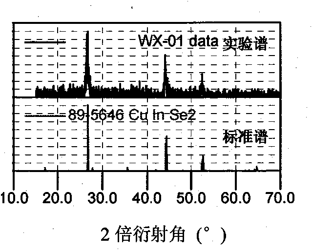
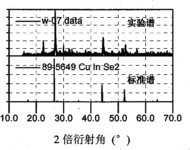
The invention discloses a method for preparing a copper-indium-selenium optoelectronic thin film material of a solar cell and belongs to the technical field of the preparation of optoelectronic thin films for solar cells. The method prepares the copper-indium-selenium optoelectronic thin film material of the solar cell by the following steps: firstly, cleaning a glass substrate; secondly, placing CuCl2.2H2O, InCl3.4H2O and SeO2 into a solvent; thirdly, adjusting the pH value of the solution to 7.5; fourthly, obtaining a precursor thin film by drying; fifthly, placing the precursor thin film sample into a closed reactor containing hydrazine hydrate and preventing the precursor thin film sample from contacting the hydrazine; and finally, obtaining a copper-indium-selenium optoelectronic thin film by drying. The method does not require high temperature and high vacuum conditions, has low requirements on instruments and is low in product cost, high in production efficiency and easy to operate. The obtained copper-indium-selenium optoelectronic thin film has excellent continuity and uniformity, and the main phase of the obtained copper-indium-selenium optoelectronic thin film is a CuInSe2 phase. The process allows for easily control of the components and structure of a target product and provides low cost and large-scale industrial production of high-performance copper-indium-selenium optoelectronic thin films.

Description

technical field [0001] The invention belongs to the technical field of photoelectric film preparation for solar cells, in particular to a copper indium selenide (CuInSe) for solar cells. 2 ) Preparation method of photoelectric thin film. Background technique [0002] With the development of society and economy, my country's total energy consumption has ranked second in the world in 2004, accounting for about 11% of the world's total energy consumption. Energy shortages and pollution caused by energy consumption have also become domestic social development Therefore, the development and utilization of clean energy is of great significance to environmental protection, sustainable economic development and building a harmonious society. Photovoltaic power generation has the advantages of safety and reliability, no noise, no pollution, less constraints, low failure rate, and easy maintenance. Solar energy, a clean, safe and environmentally friendly renewable energy, can be used. ...

Claims


Application Information

Patent Timeline
Patent Type & Authority Applications(China)
IPC IPC(8): H01L31/18
CPCY02P70/50
Inventor 刘科高项东张保议冯立明李静王志刚
Owner SHANDONG JIANZHU UNIV
Learn More