Micro-wave on-wafer testing method based on unknown material substrate

A test method, microwave technology, applied in measuring devices, measuring electrical variables, measuring resistance/reactance/impedance, etc., can solve problems such as reference impedance uncertainty, and achieve the effects of avoiding error accumulation, high test accuracy, and convenient data processing

Active Publication Date: 2010-01-27
NO 55 INST CHINA ELECTRONIC SCI & TECHNOLOGYGROUP CO LTD
View PDF0 Cites 23 Cited by
  • Summary
  • Abstract
  • Description
  • Claims
  • Application Information

AI Technical Summary

Problems solved by technology

[0010] The purpose of the present invention is to invent a test method for the test problem of the microwave component of the unknown material substrate, and solve the problem of reference impedance uncertainty during TRL calibration by testing the open circuit resonator. This method can not only extract the scattering parameters of the microwave component, but also The characteristics of the following two material substrates can be analyzed: the dielectric properties of the material can be obtained directly for a single-layer substrate; for a multi-layer substrate whose dielectric properties are unknown, the effective dielectric constant of the substrate can be obtained, with the help of The dielectric properties of unknown materials can be obtained by field analysis methods such as finite element method, moment method, and quasi-static method

Method used


Image

  • Micro-wave on-wafer testing method based on unknown material substrate
  • Micro-wave on-wafer testing method based on unknown material substrate
  • Micro-wave on-wafer testing method based on unknown material substrate

Examples


Embodiment

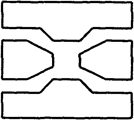
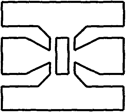
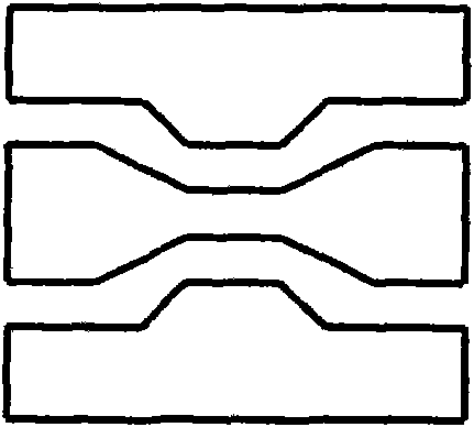
[0047] 1), the substrate structure is: 360um sapphire + 2um gallium nitride (GaN) + 0.15um barium strontium titanate (BST), the dielectric constant of the sapphire substrate is 5.5, the dielectric constant of GaN is 9.0, and the dielectric constant of BST is unknown . Manufactured by integrated circuit thin film technology figure 1 , figure 2 , image 3 , Figure 4 Medium TRL calibration kit, Figure 5 open resonator and Image 6 All patterns of the components under test adopt CPW structure, in which the line width is 120um, the gap is 25um, the length of the straight line is 250um, the lengths of the two long lines are 2090um and 3810um respectively, and the length of the open line is 1630um.

[0048] 2), use the TRL full two-port calibration function of the vector network analyzer to calibrate the microwave on-chip test system, and the calibration parts are prepared in step 1. figure 1 , figure 2 , image 3 , Figure 4 TRL calibration parts;

[0049] 3), will F...


PUM


Abstract

The invention relates to an on-wafer testing method for a micro-wave element based on an unknown material substrate. The method comprises the following steps: firstly, a TRL calibration part, an open circuit resonator and an element to be measured which are suitable for micro-wave on-wafer testing are prepared on a substrate; secondly, a micro-wave on-wafer testing system is calibrated by using a TRL calibration method; thirdly, resonation point of the open circuit resonator is tested by the calibrated micro-wave on-wafer testing system; fourthly, effective dielectric constant and transmission line impedance of the substrate are calculated according to a measured resonation point; fifthly, an S parameter of the element to be measured is measured, and reference impedance of the S parameter is the impedance obtained in the last step; and finally, a reference S parameter with 50 omega impedance is acquired by adopting a method of S parameter impedance conversion. The method has the advantages that the system impedance of the TRL calibration part can be calculated through testing the open circuit resonator; the method combined with standard TRL calibration not only can carry out on-wafer testing on the micro-wave element under the condition that the characteristic of a material is unknown, but also can be combined with a method of field analysis to calculate the real characteristic of the material.

Description

technical field [0001] The invention relates to a microwave on-chip testing method, which is suitable for calibrating and testing a system under the condition of unknown material properties, and further determining the dielectric properties of materials to obtain the scattering parameters of components. The invention is especially suitable for testing and modeling of microwave components of new material thin film substrates, and has important significance for the application of new material thin films in microwave circuits, especially microwave monolithic integrated circuits (MMIC). It belongs to the field of microwave application technology. Background technique [0002] Thin films of high dielectric constant materials (such as strontium lead titanate) and ferroelectric films (such as barium strontium titanate) have been widely used in microwave circuits. With the deepening of applications, the testing methods of dielectric properties of materials have become a research hot...

Claims


Application Information

Patent Timeline
Patent Type & Authority Applications(China)
IPC IPC(8): G01R27/26G01R27/02G01R35/00
Inventor 李辉陈效建周建军陈辰
Owner NO 55 INST CHINA ELECTRONIC SCI & TECHNOLOGYGROUP CO LTD
Why Eureka
Try Eureka