Antenna and wireless communication apparatus
一种天线、天线元件的技术,应用在天线、天线零部件、天线支持物/安装装置等方向,能够解决匹配电路损失变大、难天线谐振频率等问题,达到增大损失的效果
- Summary
- Abstract
- Description
- Claims
- Application Information
AI Technical Summary
Problems solved by technology
Method used
Image
Examples
no. 1 Embodiment approach 》
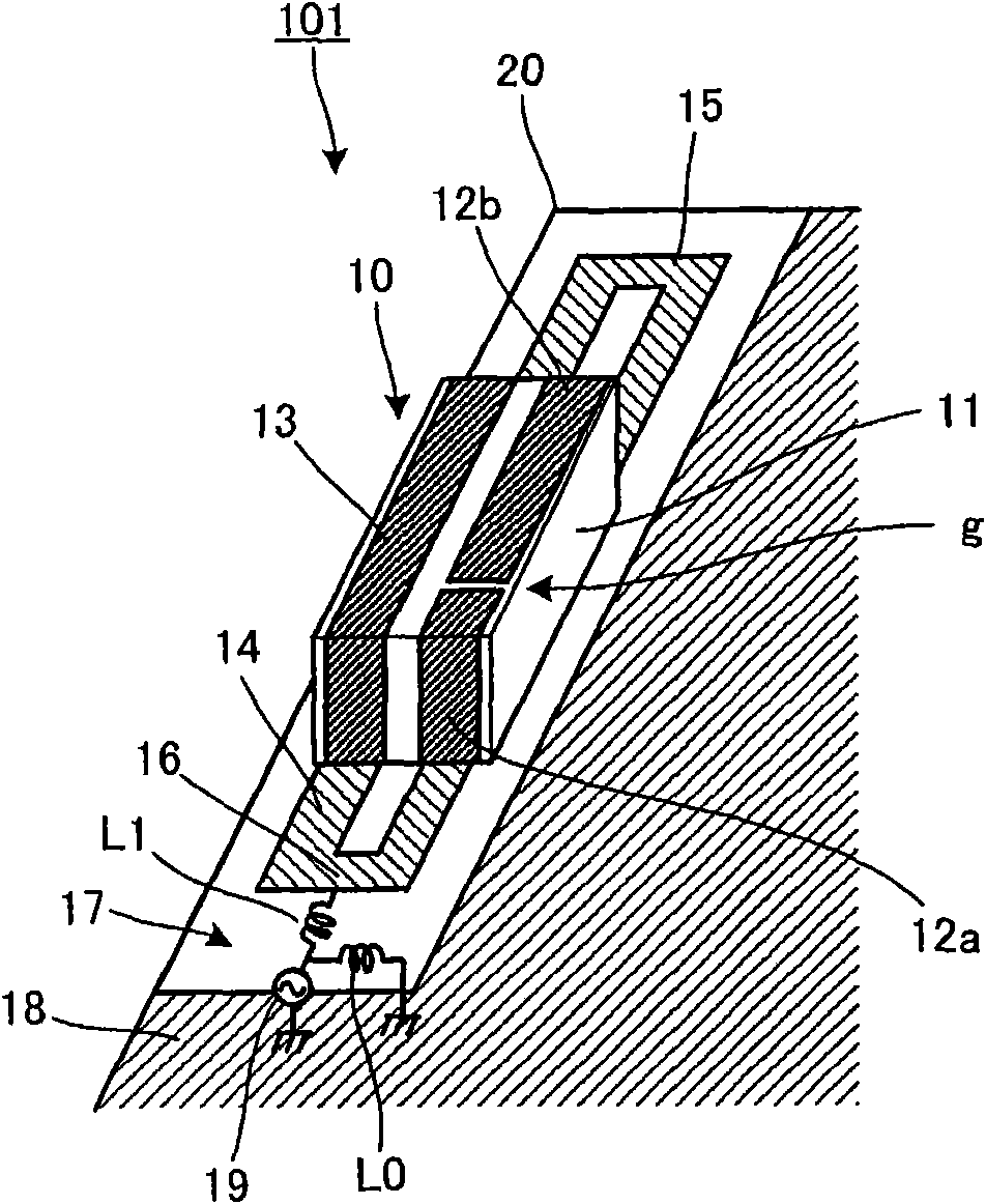
[0078] refer to Figure 2 to Figure 6 The antenna and wireless communication device according to the first embodiment will be described.
[0079] figure 2 It is a perspective view of the antenna of the first embodiment. Such as figure 2 As shown, this antenna 101 is configured by mounting the surface mount antenna element 10 on the non-ground region 17 of the mounting substrate 20 . The surface mount antenna element 10 has two linear electrodes 12 and 13 parallel to each other on the surface of a rectangular parallelepiped dielectric substrate 11, and a part of one of the electrodes 12 constitutes a capacitor portion based on a gap facing each other at a predetermined interval. g.
[0080] The first radiation electrode 14 and the second radiation electrode 15 which are respectively connected to the two linear electrodes 12 and 13 and constitute an inductor portion are formed in the non-ground region 17 of the mounting substrate 20 . Furthermore, the first radiation elec...
no. 2 Embodiment approach 》
[0088] Figure 7 It is a perspective view of the antenna of the second embodiment. and in the first embodiment figure 2 The antenna 101 shown is different in that it is provided with chip-shaped reactance elements 21 , 22 , and 23 . That is, the reactance elements 21 and 22 are surface-mounted to the first radiation electrode 14 so as to be connected in series, respectively. In addition, the second radiation electrode is composed of two linear electrode portions 15a, 15b parallel to each other, and a reactance element 23 is surface-mounted to connect predetermined positions of the two linear electrode portions 15a, 15b.
[0089] In addition, when chip inductors are used as the reactance elements 21 and 22, the inductors are connected in series with the first radiation electrode 14 on the side close to the power supply unit 19, so that the above-mentioned parallel resonant circuit and power supply can be unnecessary. The impedance matching inductor between elements 19 ( f...
no. 3 Embodiment approach 》
[0093] Figure 8 It is a perspective view of the antenna of 3rd Embodiment. and Figure 7 The antenna shown differs in the shape of the second radiation electrode 15 and the mounting structure of the reactance element 24 facing it. That is, the second radiation electrode 15 is The reactance element 24 is installed in order to connect two linear electrode portions parallel to each other.
[0094] Figure 9 yes Figure 8 A circuit diagram of antenna 103 is shown. Figure 9 (A) is an example when all the reactance elements 21, 22, and 24 are chip inductors, Figure 9 (B) is an example when the reactance elements 21 and 22 are chip inductors and 24 is a chip capacitor.
[0095] exist Figure 9 In (A) and (B), the inductors L14 a and L14 b are inductors of the first radiation electrode 14 , and the inductors L31 and L32 are inductors of the reactance elements (chip inductors) 21 and 23 . In addition, the inductor L15 is an inductor of the second radiation electrode 15 . ...
PUM
 Abstract
Description
Claims
Application Information


