Method for manufacturing metal connecting line

A manufacturing method and metal wiring technology, applied in semiconductor/solid-state device manufacturing, electrical components, circuits, etc., can solve problems such as poor reliability and low performance of metal interconnecting wires, reduce compressive stress, and ensure electronic stability. , The effect of improving the yield rate

Inactive Publication Date: 2010-02-10
GRACE SEMICON MFG CORP
View PDF3 Cites 7 Cited by
  • Summary
  • Abstract
  • Description
  • Claims
  • Application Information

AI Technical Summary

Problems solved by technology

[0011] The present invention aims to solve the problem of small bumps or peaks appearing on the metal layer due to the difference in expansion coefficients between the metal layer and the semiconductor substrate during heat

Method used


Image

  • Method for manufacturing metal connecting line
  • Method for manufacturing metal connecting line
  • Method for manufacturing metal connecting line

Examples


Embodiment Construction

[0036] In order to make the purpose and features of the present invention more obvious and understandable, the present invention will be further described by giving preferred embodiments and in conjunction with the accompanying drawings.

[0037] See image 3 , which is a flowchart of a method for manufacturing a metal wiring provided by an embodiment of the present invention. The manufacturing method includes:

[0038] S310: Provide a semiconductor substrate;

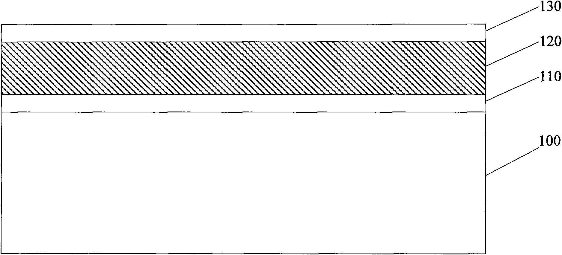
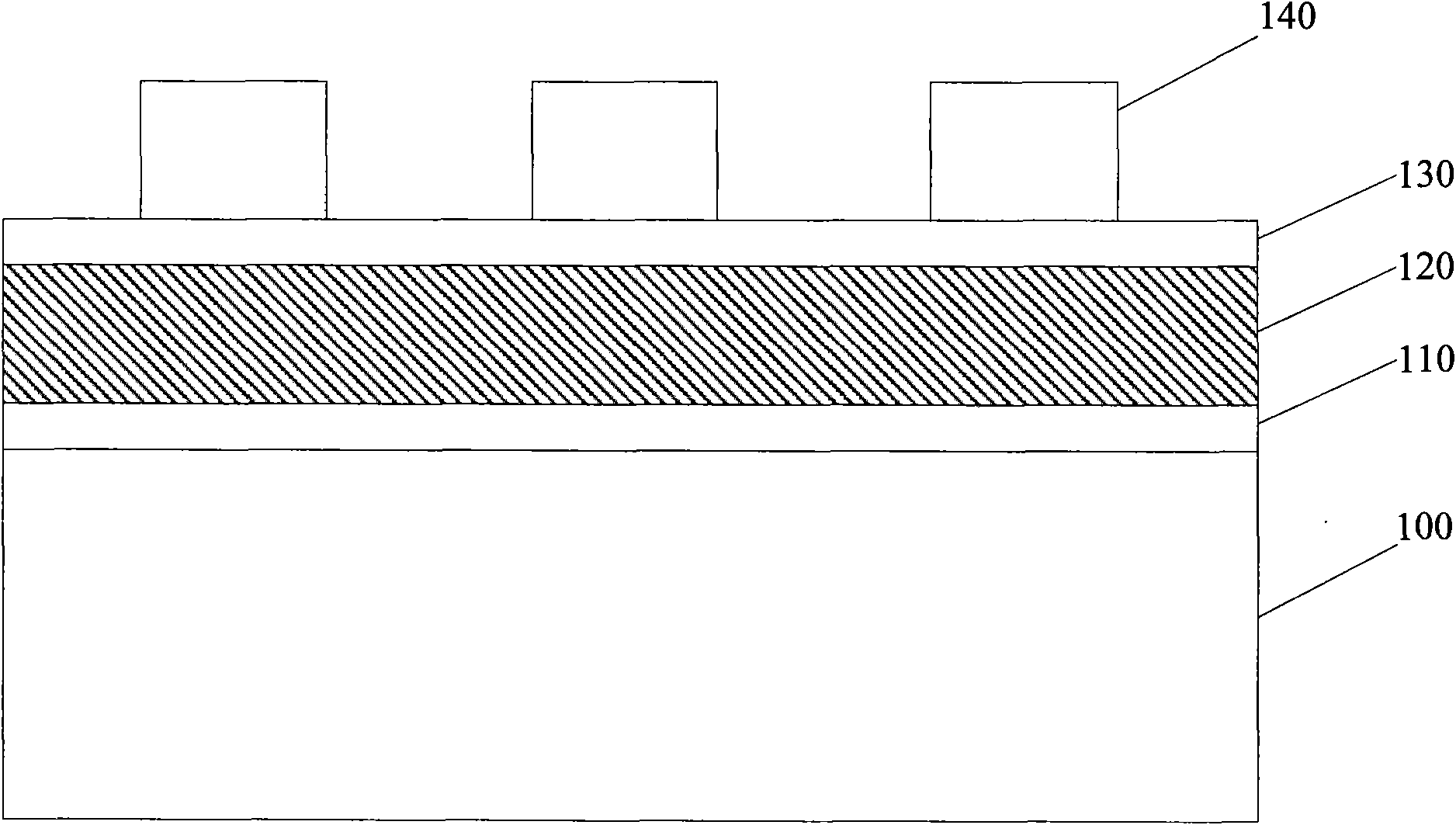
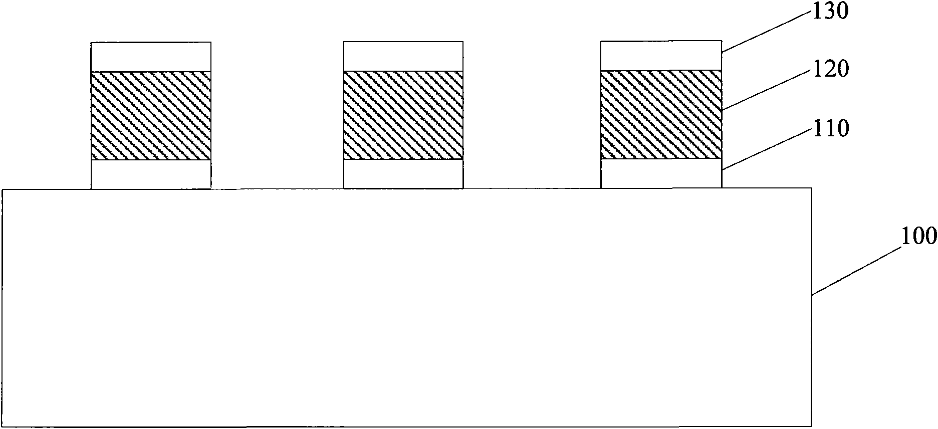
[0039] S320: forming a barrier layer on the substrate;

[0040] In this embodiment, the barrier layer is a titanium nitride (TiN) layer. There is a first adhesive layer between the barrier layer and the substrate. The first adhesion layer is a titanium (Ti) layer.

[0041] The role of the Ti layer is as an adhesion layer between the dielectric layer and the metal layer to provide better adhesion between the two layers of materials, while the TiN layer is used as a barrier layer to avoid Ti and the metal layer, suc...


PUM


Abstract

The invention discloses a method for manufacturing a metal connecting line, comprising the following steps: providing a semiconductor substrate; forming a barrier layer on the substrate; thermally processing the barrier layer; forming a metal layer on the barrier layer; forming an insulation layer and an anti-reflection layer on the metal layer; coating a photoresist layer on the anti-reflection layer; patterning the photoresist layer to define a lead pattern; and etching the anti-reflection layer, the metal layer and the barrier layer in sequence to form a lead structure. In the manufacturingmethod, a step of thermal treatment is added between the step of forming the barrier layer on the semiconductor substrate and the step of forming the metal layer so as to have an annealing effect onthe barrier layer, the barrier layer is recrystallized for hardening, pressure stress of metal lattice of the metal layer formed on the barrier layer sequentially caused by thermal treatment such as annealing, and the like is reduced, and embossment or projection of the metal layer can not occur, thereby ensuring the electronic stability of the manufactured devices and improving the yield of products.

Description

technical field [0001] The invention relates to the field of semiconductor manufacturing, in particular to a method for manufacturing metal wiring. Background technique [0002] The manufacture of semiconductor integrated circuits is an extremely complex process, the purpose of which is to reduce the various electronic components and circuits required for a specific circuit on a small area substrate. In recent years, with the development of semiconductor integrated circuit manufacturing technology, the number of components contained in the chip has been increasing, and the size of the components has been shrinking with the increase in integration. The surface of the chip is gradually unable to provide enough area to make the required Inner wires. In order to meet the new requirements, the design of metal conduction with more than two layers has gradually become the method that many integrated circuits must adopt, especially some products with more complex functions, such as...

Claims


Application Information

Patent Timeline
IPC IPC(8): H01L21/768H01L21/3105
Inventor 汪洋王立兵康军
Owner GRACE SEMICON MFG CORP
Why Eureka
Try Eureka