Impurity diffusion process in semiconductor device preparation process

A preparation process and impurity diffusion technology, applied in semiconductor/solid-state device manufacturing, electrical components, circuits, etc., can solve problems such as affecting chip parameters and performance, large process deviation, and deterioration of junction characteristics, and improve product quality consistency. , saving power and water consumption, and improving the effect of device contamination

Active Publication Date: 2019-04-23
NO 47 INST OF CHINA ELECTRONICS TECH GRP
View PDF5 Cites 3 Cited by
  • Summary
  • Abstract
  • Description
  • Claims
  • Application Information

AI Technical Summary

Problems solved by technology

But this method also has some deficiencies. There are three main points: First, the process time is long. Taking the base diffusion process as an example, the square resistance reaches 5Ω / □, and the junction depth is about 10 μm. The overall process time will reach more than ten hours. It will affect the production capacity and progress for a long time, and the process deviation will be relatively large; secondly, there are more temperature rises and falls. After the step, it stays outside for a long time, which is easy to introduce contamination problems. Even if the cleaning operation is performed, it will also cause problems such as surface leakage, which will affect the parameters and performance of the chip.

Method used


Image

  • Impurity diffusion process in semiconductor device preparation process
  • Impurity diffusion process in semiconductor device preparation process
  • Impurity diffusion process in semiconductor device preparation process

Examples


Embodiment 1

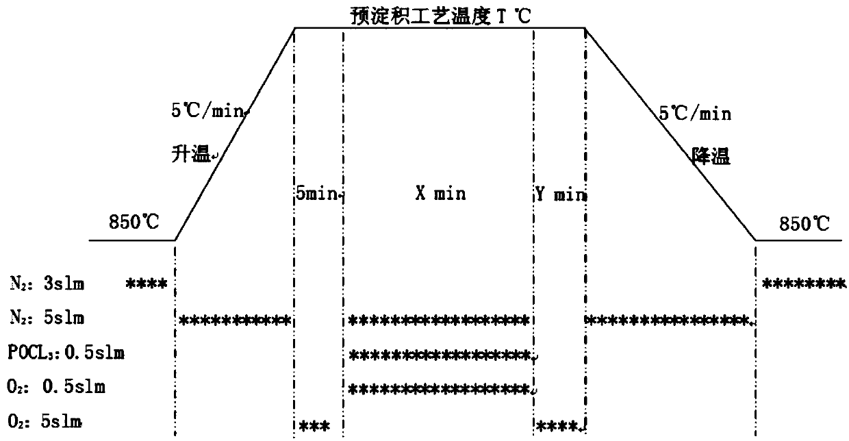
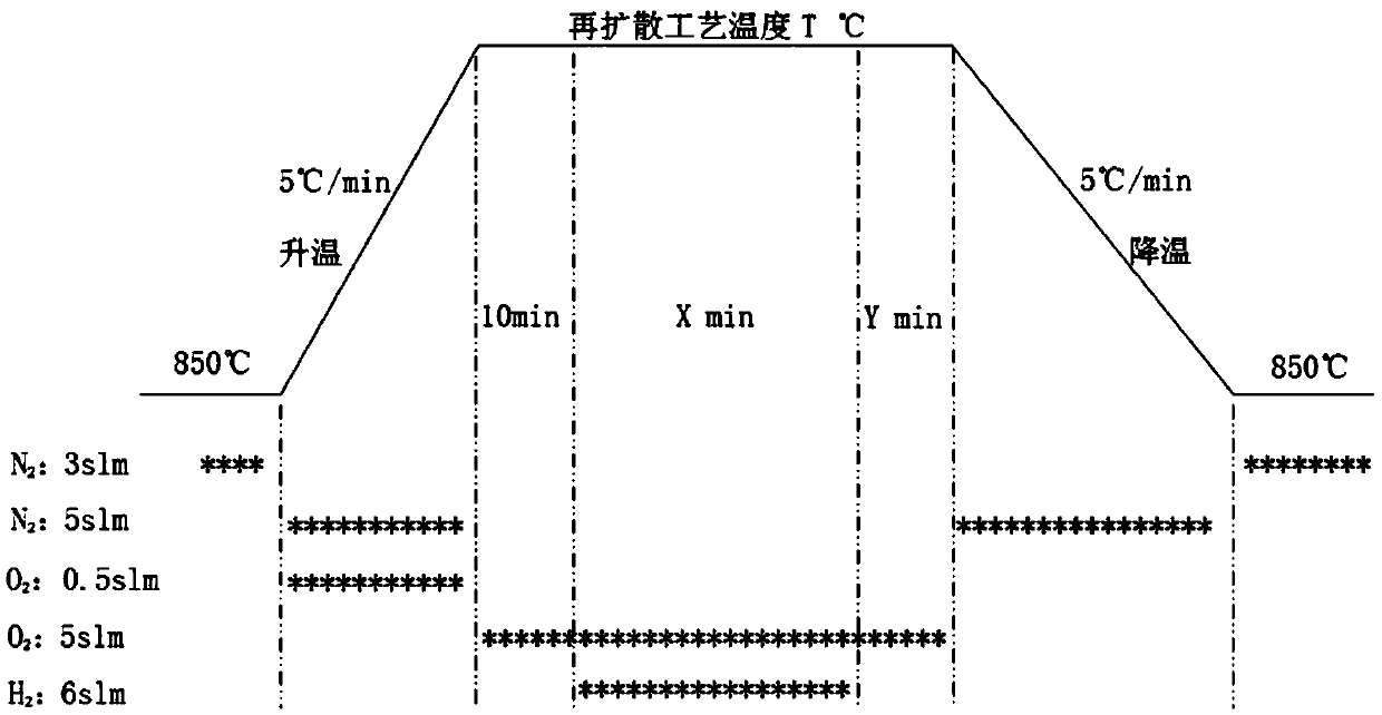
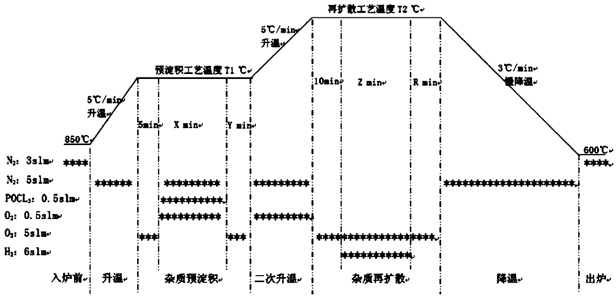
[0045] Present embodiment is the POCl of a certain product that adopts technology of the present invention to carry out 3 Diffusion of impurity phosphorus as a dopant source, the process is as follows:

[0046] 1. Clean the silicon wafer for 1.5 hours;

[0047] 2. According to the process curve ( image 3 ), wherein T1=1050°C, X=40 minutes, Y=0, T2=1140°C, Z=10 minutes, R=40 minutes, the whole process is about 5 hours, and the whole optimized process is about 6.5 hours.

[0048]Parameter comparison, the main parameters include RS (surface resistance), XJ junction depth, TOX oxide layer thickness. In the process of the process, place the front, middle and back three position measurement pieces in the constant temperature area, respectively mark 1#, 2# and 3#, to determine the parameter distribution, and test the silicon chip when performing the RS surface resistance and TOX parameter test The parameter values ​​of the upper, middle, lower, left, and right positions are shown...


PUM


Abstract

The invention discloses an impurity diffusion process in a semiconductor device preparation process, and belongs to the technical field of semiconductor device manufacturing. The process first performs an impurity pre-deposition process, and then a diffusion furnace is heated to a re-diffusion temperature T2 at a rate of 5 DEG C / min under a mixed atmosphere of nitrogen and oxygen; the impurities are re-diffused, and finally the diffusion furnace is placed under a nitrogen atmosphere of 5 slm to be cooled to below 600 DEG C at a rate of 3 DEG C / min, and a silicon wafer is taken put and then naturally cooled. The impurity pre-deposition and diffusion process in the furnace are completed at one time to avoid the influence of repeated lifting and lowering temperature on product parameters andperformance and shorten a large amount of process time.

Description

technical field [0001] The invention relates to the technical field of semiconductor device preparation, in particular to an impurity diffusion process in the semiconductor device preparation process. Background technique [0002] The diffusion process is to dope a certain amount of certain impurities into the semiconductor material (such as silicon crystal) to change its electrical properties, and make the amount, distribution and depth of the doped impurities meet the requirements, so as to form the device function. At present, the pre-deposition plus re-diffusion process is commonly used, which is also the most widely used preparation method in the semiconductor diffusion process. Pre-deposition is to pass the gas containing the required impurities through the surface of the silicon wafer at high temperature, so that the impurities are decomposed from the compound, and these impurities are concentrated in a thinner layer on the surface of the silicon surface. The specific...

Claims


Application Information

Patent Timeline
Patent Type & Authority Applications(China)
IPC IPC(8): H01L21/225H01L21/228
CPCH01L21/2252H01L21/228Y02P70/50
Inventor 吴会利刘旸
Owner NO 47 INST OF CHINA ELECTRONICS TECH GRP
Why Eureka
Try Eureka