Check patentability & draft patents in minutes with Patsnap Eureka AI!

Mask plate for exposure of the same layer and multi-exposure method thereof

A technology of multiple exposure and mask plate, applied in the field of multiple exposure, can solve the problems of decreased alignment error and exposure efficiency, and achieve the effect of reducing alignment error and reducing process time

Inactive Publication Date: 2010-03-03
GRACE SEMICON MFG CORP
View PDF0 Cites 6 Cited by
  • Summary
  • Abstract
  • Description
  • Claims
  • Application Information

AI Technical Summary

Problems solved by technology

[0004] The technical problem to be solved by the present invention is to avoid the problems of decreased alignment error and decreased exposure efficiency caused by changing the mask plate in the multiple exposure method, and propose a mask plate for exposure of the same layer and its multiple exposure method

Method used


Image

  • Mask plate for exposure of the same layer and multi-exposure method thereof
  • Mask plate for exposure of the same layer and multi-exposure method thereof
  • Mask plate for exposure of the same layer and multi-exposure method thereof

Examples


Embodiment Construction

[0014] In order to make the object, technical solution and advantages of the present invention clearer, the present invention will be further described in detail below in conjunction with the accompanying drawings.

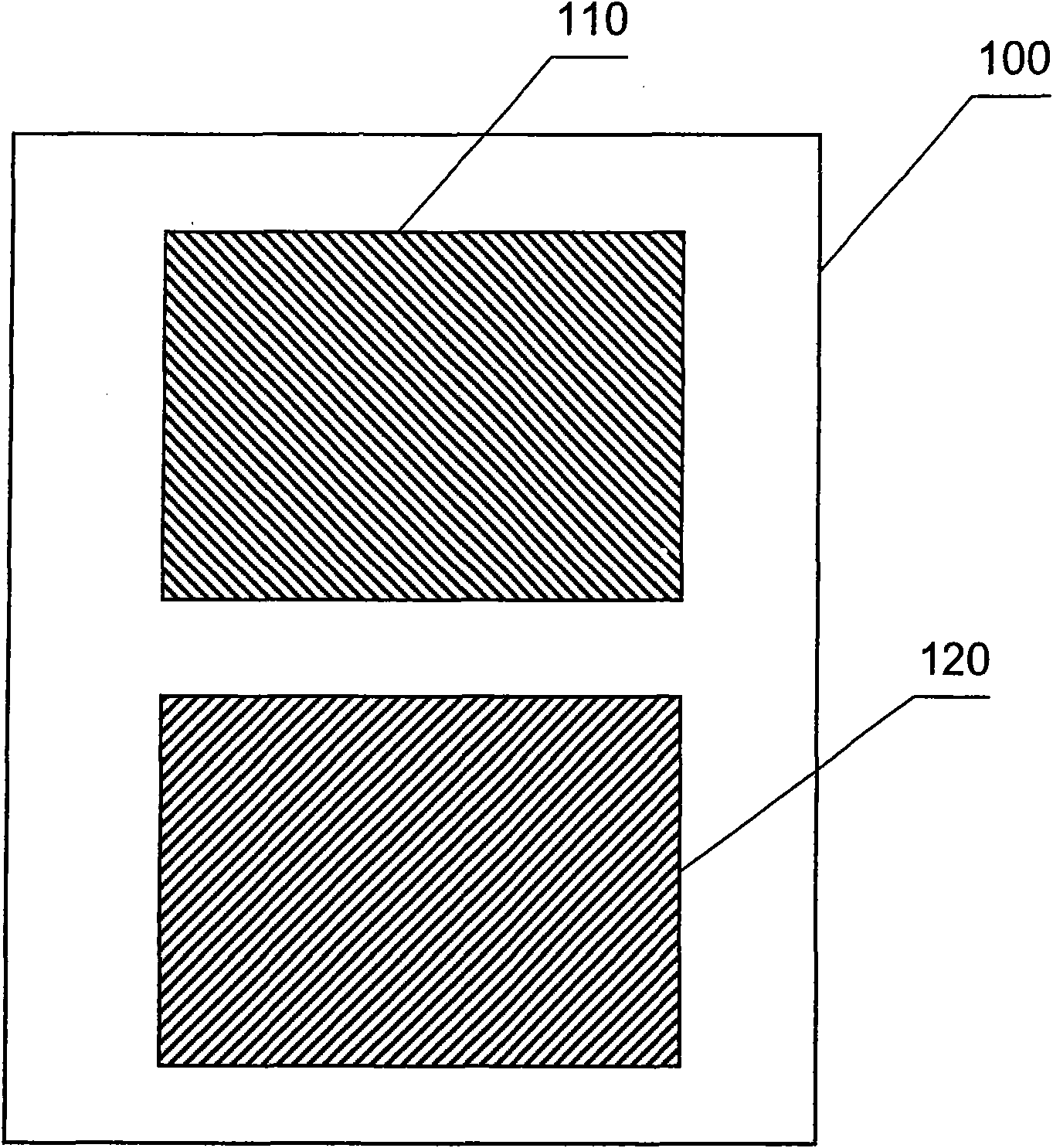
[0015] figure 1 Shown is a schematic diagram of the mask plate according to the first embodiment of the present invention. Such as figure 1 As shown, the mask plate 100 includes a first mask plate pattern area 110 and a second mask plate pattern area 120, both of which are used to pattern the same layer of the chip, the first mask plate The pattern area 110 and the second mask pattern area 120 are independent from each other, that is, one of the mask pattern areas can be used alone to expose the photoresist on the wafer. When exposing, the exposure conditions used in the first mask pattern area 110 and the second mask pattern area 120 are different, for example, because the pattern density of the first mask pattern area 110 is higher than that of the second mask...


PUM


Abstract

The invention provides a mask plate for exposure of the same layer and a multi-exposure method thereof, belonging to the photoetching technical field. The method comprises the following steps: the mask plate for multi-exposure at the same layer is manufactured on the same mask plate so that the mask plate comprises a plurality of mutually-independent mask plate graph regions; and a mask plate bearing table controls movement of the mask plate during multiple exposure so that different mask plate graph regions are selected for each exposure and different exposure conditions are selected in eachexposure. In the multi-exposure method, change of the mask plate and realignment of a wafer are not required, thus reducing alignment error and decreasing process time of exposure.

Description

technical field [0001] The invention belongs to the technical field of photolithography, and in particular relates to a mask for making a plurality of mutually independent mask pattern areas of the same layer and a multiple exposure method for exposing by using the mask. Background technique [0002] With the rapid development of semiconductor manufacturing technology, the chip runs faster and faster, the power consumption is lower and lower, and the chip is developing towards small size, high integration and multi-function. Especially with the development of SOC (system on chip) and other technologies, chips are becoming more and more complex, and the functional areas in each layer of the chip are relatively clear. The difference in functional areas in each layer of graphics leads to obvious differences in exposed graphics. The exposure conditions required are also different. Therefore, a multiple exposure method is proposed in the prior art to expose different functional ...

Claims


Application Information

Patent Timeline
Patent Type & Authority Applications(China)
IPC IPC(8): G03F1/14G03F7/20G03F1/00
Inventor 陈蕾鲍晔胡林周孟兴
Owner GRACE SEMICON MFG CORP
Features
  • R&D
  • Intellectual Property
  • Life Sciences
  • Materials
  • Tech Scout
  • Unparalleled Data Quality
  • Higher Quality Content
  • 60% Fewer Hallucinations
Learn More