Flip-chip packaging method and structure

A technology of packaging structure and packaging method, which is applied in the manufacturing of electrical components, electric solid-state devices, semiconductor/solid-state devices, etc., can solve the problems of increasing the difficulty of primer, shrinking solder mask openings, and difficulty in printing solder materials.

Inactive Publication Date: 2010-03-03
UNIMICRON TECH CORP
View PDF0 Cites 9 Cited by
  • Summary
  • Abstract
  • Description
  • Claims
  • Application Information

AI Technical Summary

Problems solved by technology

However, as the bump pitch becomes smaller and smaller, the solder pad must also be reduced accordingly, and the solder mask opening is also reduced, which causes difficulties in printing solder materials and leads to a decrease in yield.
On the other hand, if the NSMD design is adopted, although the solder balls of the chip can be directly combined with the solder pads on the carrier board by enlarging the solder resist opening, and the step of printing solder materials is omitted, however, such an approach will cause The gap between the chip and the solder mask layer is too small, which increases the difficulty of subsequent underfill coating

Method used


Image

  • Flip-chip packaging method and structure
  • Flip-chip packaging method and structure
  • Flip-chip packaging method and structure

Examples


Embodiment Construction

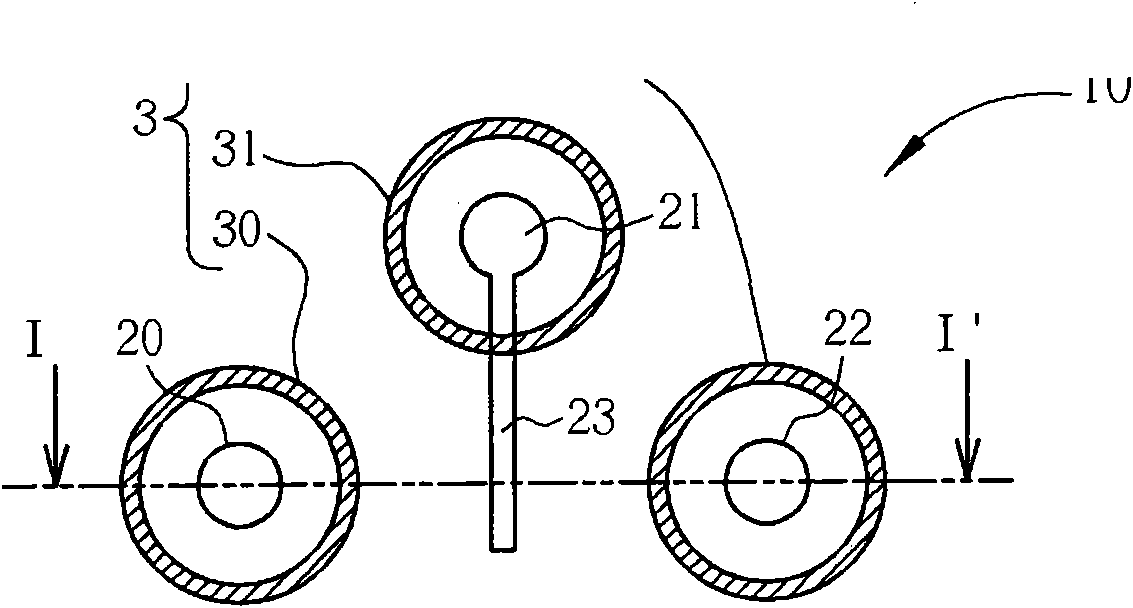
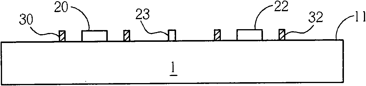
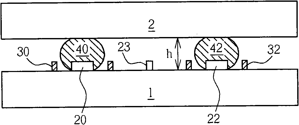
[0027] see figure 1 and figure 2 ,in figure 1 It is a schematic top view of a flip-chip solder resist pattern according to an embodiment of the present invention, figure 2 for along figure 1 The cross-sectional schematic diagram drawn by the middle tangent line I-I'. Such as figure 1 and figure 2 As shown, a substrate 1 is provided at first, and then metal patterns 20, 21, 22 and 23 are formed in a predetermined area 10 of the substrate 1, wherein the metal patterns 20, 21, 22 are metal pads for contact with the tin on the chip. Balls or bumps are combined, and the metal pattern 23 is a metal thin wire connected to the metal pattern 21 .

[0028] According to an embodiment of the present invention, the substrate 1 may be a plastic substrate or a ceramic substrate, etc., and a multi-layer interconnection structure (not shown) may be formed therein. The metal patterns 20 , 21 , 22 and 23 may be made of copper, other metals or metal alloy materials. The methods for for...


PUM


Abstract

The invention discloses flip-chip packaging method and structure. The method comprises the steps: providing a base plate which is provided with a welding pad pattern; forming an annular welding-prooffigure on the base plate around the welding pad pattern; aligning a convex block of a flip-chip with the welding pad pattern; combining the convex block with the welding pad pattern and filling a filling material between the flip-chip and the base plate. The invention has an innovative welding-proof figure design of the flip-chip, has the advantages of SMD design and NSMD design and also solves the problem of subsequent primer application.

Description

technical field [0001] The invention relates to the technical field of flip-chip packaging, in particular to a flip-chip packaging structure and a flip-chip packaging method with an innovative flip-chip solder-proof graphic design. Background technique [0002] With the demand for thinner and smaller electronic products, the development of packaging technology is also moving towards modularization and large-scale integration to save the volume of packaging components. In the development of packaging technology, the chip bonding technology has developed from the past wire bonding technology and tape automated bonding (TAB) to the current flip chip (flip-chip) bonding technology. [0003] Packaging technology usually requires the use of a chip carrier, which is mainly used to connect the chip and the motherboard (motherboard), and has the functions of protecting the chip and cooling. Generally speaking, a chip carrier is formed by laminating multiple layers of patterned wire ...

Claims


Application Information

Patent Timeline
Patent Type & Authority Applications(China)
IPC IPC(8): H01L21/50H01L21/60H01L21/56H01L23/488H01L23/498H01L23/31H01L23/10
Inventor 范智朋
Owner UNIMICRON TECH CORP
Why Eureka
Try Eureka