Process for manufacturing monocrystalline silicon solar cell texture with low surface reflectivity

A solar cell and manufacturing process technology, applied in the field of solar energy applications, can solve the problems of restricting solar cell efficiency, large light reflection loss, weakened long-wave absorption, etc., and achieves the effects of simple manufacturing process, low surface reflectivity, and low price.

Active Publication Date: 2010-03-03
ZHEJIANG UNIV
View PDF0 Cites 30 Cited by
  • Summary
  • Abstract
  • Description
  • Claims
  • Application Information

AI Technical Summary

Problems solved by technology

When the silicon wafer becomes thinner, the absorption of light, especially the long-wave absorption, will be weakened, and the excited photogenerated carriers will decrease, which will reduce the photoelectric conversion efficiency of the solar cell.
However, the existing conventional texture making process is to form a pyramid texture structure by alkali reaction. The average reflectance in the visible light band is generally above 10%, and the reflection loss of light is relatively large, which restricts the further improvement of solar cell efficiency.

Method used


Image

  • Process for manufacturing monocrystalline silicon solar cell texture with low surface reflectivity
  • Process for manufacturing monocrystalline silicon solar cell texture with low surface reflectivity
  • Process for manufacturing monocrystalline silicon solar cell texture with low surface reflectivity

Examples


Embodiment 1

[0013] 1) Put a silicon wafer with a thickness of 180±5μm and a size of 20mm×20mm into a 20mt% KOH solution, and react at 80°C for 2min to remove the surface damage of the silicon wafer;

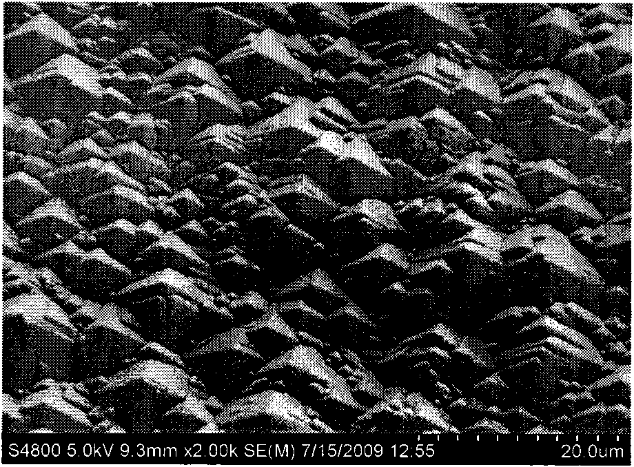
[0014] 2) Put the cleaned silicon chip into a mixed solution of KOH and isopropanol, wherein the concentration of KOH is 3mt%, and the concentration of isopropanol is 8vol%, react at 80°C for 60min, and form on the surface of the silicon chip Pyramid structures of uniform size (see figure 1 );

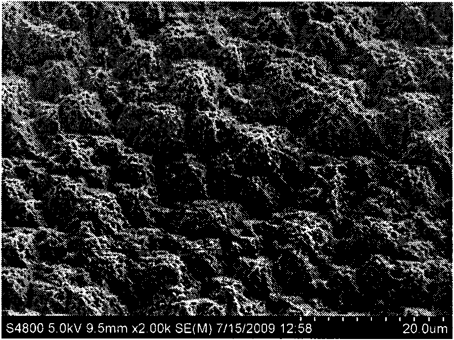
[0015] 3) Put the silicon chip with a pyramid structure in step 2) into a polytetrafluoroethylene kettle filled with corrosive liquid, seal it, and react at 50°C for 30 minutes, the corrosive liquid is 10mol / L HF+0.2mol / L Fe (NO 3 ) 3 The mixed solution forms porous silicon on the surface of the pyramid, see figure 2 , the porous structure on the surface of the pyramid structure is conducive to the further absorption of incident light. The low surface reflectance of the monocrystalline silicon s...

Embodiment 2

[0017] 1) Put a silicon wafer with a thickness of 180±5μm and a size of 20mm×20mm into a 20mt% KOH solution, and react at 80°C for 2min to remove the surface damage of the silicon wafer;

[0018] 2) Put the cleaned silicon chip into a mixed solution of KOH and isopropanol, wherein the concentration of KOH is 3mt%, and the concentration of isopropanol is 8vol%, react at 80°C for 60min, and form on the surface of the silicon chip Pyramid structure of uniform size;

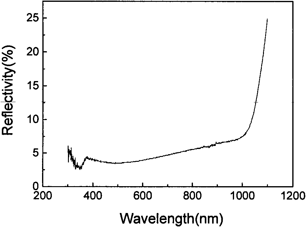
[0019] 3) Put the silicon chip with a pyramid structure in step 2) into a polytetrafluoroethylene kettle filled with corrosive liquid, seal it, and react at 10°C for 60 minutes, the corrosive liquid is 5mol / L HF+0.4mol / L Fe (NO 3 ) 3 The mixed solution forms porous silicon on the surface of the pyramid to obtain the textured surface of the monocrystalline silicon solar cell with low surface reflectance, and the average reflectance is 8.2% in the visible light range of 400nm to 800nm.

Embodiment 3

[0021] The size of the original silicon wafer (180±5μm) used is 20mm×20mm. First, use 20mt% KOH solution to remove the surface damage of the silicon wafer, and react at 80°C for 2min; ℃ for 60min, then in 15mol / L HF+0.1mol / L Fe(NO 3 ) 3 When the reaction time in the solution is 10 minutes, the average reflectance obtained in the range of visible light (400nm-800nm) is 6.9%.

[0022] 1) Put a silicon wafer with a thickness of 180±5μm and a size of 20mm×20mm into a 20mt% KOH solution, and react at 80°C for 2min to remove the surface damage of the silicon wafer;

[0023] 2) Put the cleaned silicon chip into a mixed solution of KOH and isopropanol, wherein the concentration of KOH is 3mt%, and the concentration of isopropanol is 8vol%, react at 80°C for 60min, and form on the surface of the silicon chip Pyramid structure of uniform size;

[0024] 3) Put the silicon chip with a pyramid structure in step 2) into a polytetrafluoroethylene kettle filled with corrosive liquid, seal ...


PUM

PropertyMeasurementUnit
thicknessaaaaaaaaaa
reflectanceaaaaaaaaaa

Abstract

The invention discloses a process for manufacturing monocrystalline silicon solar cell texture with low surface reflectivity, comprising the steps of: washing silicon slices to remove damage on surfaces of the silicon slices; putting the washed silicon slices into a mixed solution formed by KOH and isopropanol to form a pyramid structure with equal size on the surfaces of the silicon slices; and putting the silicon slices with pyramid structure into the mixed solution formed by HF and Fe(NO3)3 for corrosion so as to form porous silicon on surface of the pyramid structure. The manufacturing process of the invention is simple, and the corrosion liquid is inexpensive; and the manufacturing process is compatible with the prior art and the surface reflectivity of the processed silicon slices islow, and can be less than 5 percent.

Description

technical field [0001] The invention relates to a fabricating process for thin monocrystalline silicon solar cells, in particular to a fabricating process for monocrystalline silicon solar cells with low surface reflectivity, and belongs to the field of solar energy applications. Background technique [0002] At present, crystalline silicon is still the most important solar cell material, with a market share of about 90%. More than 50% of battery production costs come from silicon materials. The thickness of monocrystalline silicon wafers for solar cells has been around 200 μm, and is developing towards 150 μm or even thinner. When the silicon wafer becomes thinner, the absorption of light, especially the long-wave absorption, will be weakened, and the excited photo-generated carriers will decrease, which will reduce the photoelectric conversion efficiency of the solar cell. However, the existing conventional texture making process is to form a pyramid texture structure by...

Claims


Application Information

Patent Timeline
Patent Type & Authority Applications(China)
IPC IPC(8): H01L31/18
CPCY02P70/50
Inventor 汪雷肖俊峰杨德仁
Owner ZHEJIANG UNIV
Why Eureka
Try Eureka