Manufacturing method for printed wiring board with dense disk holes

A technology for printed circuit board and manufacturing method, which is applied in the directions of printed circuit, printed circuit manufacturing, and the formation of electrical connection of printed components, etc., can solve the problems of excessive product size change, difficulty in resin grinding, and uneven reduction of copper thickness on the board surface. , to achieve the effect of solving the problem that the plug hole is not full and the difficulty of resin grinding

Inactive Publication Date: 2010-03-03
DONGGUAN MEADVILLE CIRCUITS
View PDF0 Cites 40 Cited by
  • Summary
  • Abstract
  • Description
  • Claims
  • Application Information

AI Technical Summary

Problems solved by technology

[0006] Another object of the present invention is to provide a method for manufacturing a printed circuit board with high-density disk holes, which uses abrasive belt and four-axis non-woven grinding techno

Method used


Image

  • Manufacturing method for printed wiring board with dense disk holes

Examples


Embodiment Construction

[0030] In order to further illustrate the technical means adopted by the present invention and its effects, the following describes in detail in conjunction with preferred embodiments of the present invention and accompanying drawings.

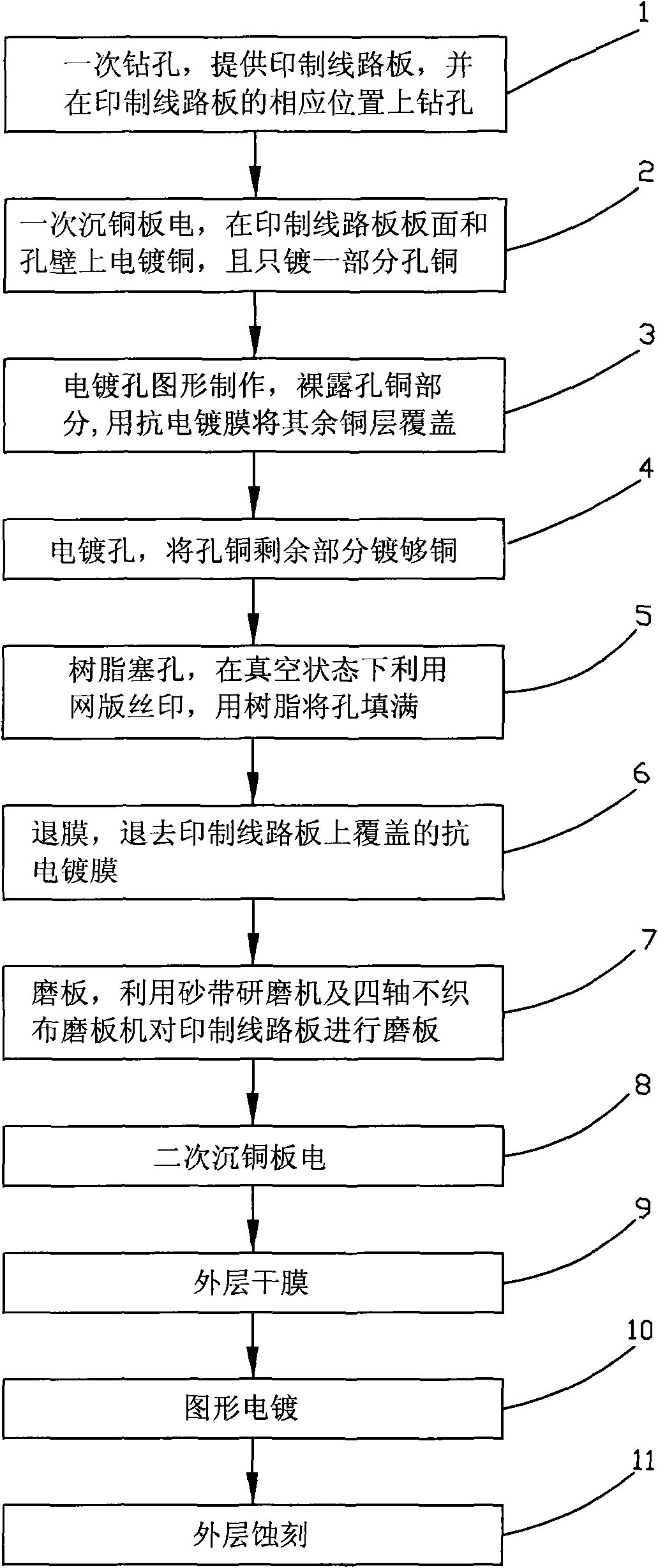
[0031] Such as figure 1 As shown, it is a schematic flow chart of the manufacturing method of the printed circuit board with the hole in the high density disc of the present invention, the method comprises:

[0032] Step 1, drilling holes once, providing a printed circuit board, and drilling holes at corresponding positions on the printed circuit board.

[0033] Step 2, a copper sinking electroplating, electroplating copper on the surface of the printed circuit board and the hole wall of the drilled hole, and electroplating only a part of the hole copper in the hole wall. In this embodiment, only about 10um of hole copper is electroplated in the hole wall at a time.

[0034] Step 3, making the electroplating hole pattern, exposing the copper...


PUM

PropertyMeasurementUnit
Thicknessaaaaaaaaaa
Thicknessaaaaaaaaaa

Abstract

The invention relates to a manufacturing method for a printed wiring board with dense disk holes, comprising the steps of: 1 once boring a hole, 2 once plating copper on the board surface and a wall of a hole of a printed wiring board and only partially plating the wall of the hole, 3 making a pattern of plating hole, 4 plating copper on the part of the hole which is not plated, 5 filling the holewith resin by adopting silk-screen in vacuum, 6 withdrawing a film, 7 grinding a printed wiring board with an abrasive band grinding machine and a four-axle unwoven cloth graining machine, 8 secondarily plating copper on the board, 9 drying a film on the outer layer, 10 plating the pattern and 11 etching the outer layer. The invention manufactures the products with dense disk holes with a line width and line-spacing of 4/4mil, by once plating copper on a 10um hole. The problems of partially filled tap-hole, hollow resin, resin foam, etc., are efficiently solved by adopting the vacuum silk-screen technique and the problems of difficult grinding of resin, sunken resin, unevenly cutting of the copper on the board surface, etc., are efficiently solved by grinding with abrasive band and four-axle unwoven cloth graining technique.

Description

technical field [0001] The invention relates to a method for manufacturing a printed circuit board, in particular to a method for manufacturing a printed circuit board with holes in a highly dense disk. Background technique [0002] With the rapid development of electronic technology, electronic products are developing in the direction of miniaturization, portability, multi-function, high integration and high reliability, and the packaging of semiconductor components is also developing rapidly towards multi-pin and fine-pitch, which requires corresponding requirements. The printed circuit boards of semiconductor components not only need to be multi-layered, and the area that can be routed can be increased by increasing the number of layers, but also need to be small, lightweight and high-density. In order to meet the needs of high wiring density placed in more and more functions of electronic products, through holes or stacked hole structures are mainly used to connect the c...

Claims


Application Information

Patent Timeline
IPC IPC(8): H05K3/42H05K3/18
Inventor 梁敬业唐明阳雷明权
Owner DONGGUAN MEADVILLE CIRCUITS
Why Eureka
Try Eureka