Semiconductor integrated circuit

A technology of integrated circuits and semiconductors, applied in the field of semiconductor integrated circuits, can solve problems such as inability to change comb teeth, difficult-to-comb capacitors, and ensure capacitor accuracy

Inactive Publication Date: 2010-03-03
PANASONIC CORP
View PDF1 Cites 4 Cited by
  • Summary
  • Abstract
  • Description
  • Claims
  • Application Information

AI Technical Summary

Problems solved by technology

on the other hand, figure 2 In the traditional comb-shaped capacitor shown, the size of the capacitor forming surface is determined by the height h0 of the comb-tooth portion × the length L0 of the comb-tooth portion. However, since the height h0 of the comb-tooth portion...

Method used


Image

  • Semiconductor integrated circuit
  • Semiconductor integrated circuit
  • Semiconductor integrated circuit

Examples


Embodiment 1

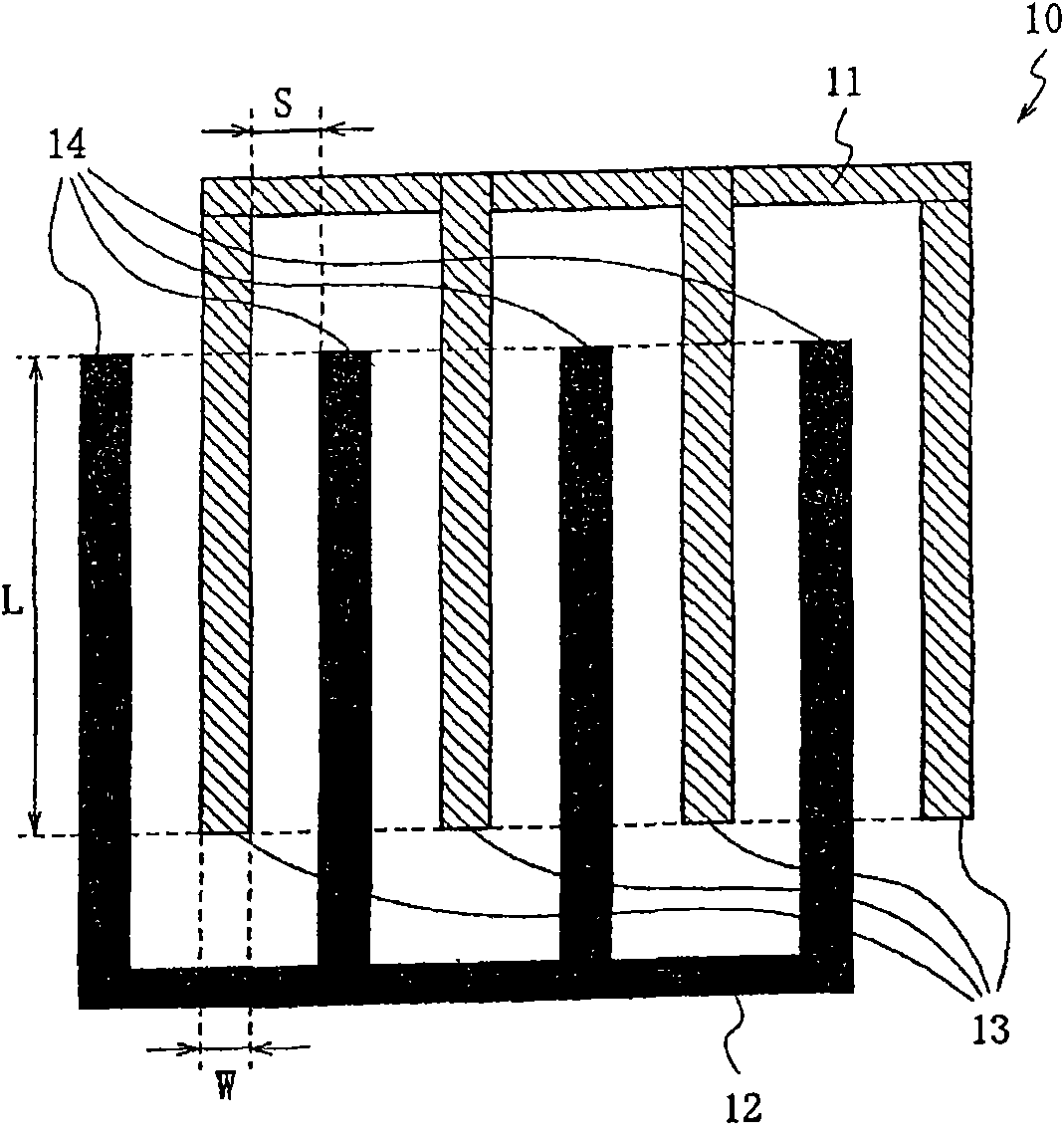
figure 1 The structure of the analog macro comb capacitor mounted on the semiconductor integrated circuit of the first embodiment is shown. Here, an analog macro refers to a circuit composed of a plurality of analog elements. figure 1 The comb-shaped capacitor 10 shown has a comb-shaped electrode 11 and an electrode 12, and the comb-tooth portion 13 of the electrode 11 and the comb-tooth portion 14 of the electrode 12 are engaged to form, so that the comb-tooth portion 13 of the electrode 11 and the comb of the electrode 12 The teeth 14 are alternately arranged in parallel. Here, the electrode 11 and the electrode 12 respectively have four comb-tooth portions, but the present invention is not limited thereto, and the number of comb-tooth portions of the electrode 11 and the electrode 12 of the comb capacitor can be arbitrary.

[0052]

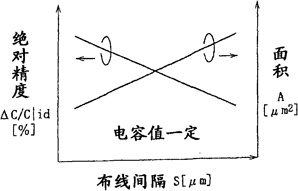
The first embodiment is characterized in that the comb-tooth interval S of the comb capacitor is set differently according to the absolute ...

Embodiment 2

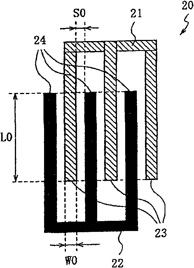
The semiconductor integrated circuit of the second embodiment is characterized in that a plurality of analog macros having a plurality of comb capacitors are mounted, and the comb-tooth interval S of each comb capacitor of each analog macro is expressed as the distance between the adjacent comb capacitors. The relative accuracy of the difference between the capacitance values ​​is set to be different.

[0118]

Such as figure 1 As shown, each comb-shaped capacitor has a comb-shaped electrode 11 and an electrode 12, and the comb-tooth portion 13 of the electrode 11 is formed by engaging with the comb-tooth portion 13 of the electrode 12. As a result, the comb-tooth portion 13 of the electrode 11 and the comb of the electrode 12 The teeth i4 are alternately arranged in parallel.

[0119]

If the vacuum dielectric constant is ε0, the relative permittivity of the oxide film is εox, the ideal capacitance value is C, and the thickness of the comb tooth portion is h, the interlock...

Embodiment 3

The semiconductor integrated circuit of the third embodiment is characterized in that it is equipped with an analog macro having a plurality of analog circuit blocks including a plurality of comb-shaped capacitors, and the comb-tooth portion intervals of the comb-shaped capacitors are adjusted for each analog circuit block. vary.

[0151]

Figure 12 It is a block diagram showing a configuration example of an analog macro having a plurality of analog circuit blocks including comb capacitors. Figure 12 Among them, the analog macro 121 has five analog circuit blocks with different functions. Since the functions of the analog circuit blocks 1201, 1202, 1203, 1204, and 1205 are different, the required capacitance accuracy is also different. Therefore, each analog circuit block has a comb capacitance with a different comb-tooth interval S according to the required capacitance absolute accuracy or relative accuracy. Therefore, a high-density comb capacitor with a narrow comb-too...


PUM

PropertyMeasurementUnit
Capacitanceaaaaaaaaaa

Abstract

A semiconductor integrated circuit is characterized in that it comprises analog macros each having a comb capacitor (10), each comb capacitor (10) is composed of comb-shaped electrodes (11, 12), the comb tooth portions (13) of the electrode (11) and the comb tooth portions (14) of the electrode (12) are so interdigitized that the comb tooth portions (13) and the comb tooth portions (14) are alternated and parallel to one another, and the tooth portion intervals (S) are varied according to the absolute accuracy indicating the difference between the actual capacitance and the ideal capacitance or the relative accuracy indicating the differencebetween the capacitances of the adjacent comb capacitors. A high-accuracy analog macro comprising a comb capacitor whose high capacitance accuracy is ensured and a semiconductor integrated circuit comprising highly-integrated analog macros are provided.

Description

technical field [0001] The present invention relates to a semiconductor integrated circuit, and more particularly, to a semiconductor integrated circuit equipped with an analog circuit having comb capacitors. Background technique [0002] Hereinafter, a semiconductor integrated circuit mounted with an analog circuit having conventional comb capacitors will be described (for example, Patent Document 1). [0003] figure 2 It is an explanatory diagram of an example of a conventional comb capacitor shown in Patent Document 1. figure 2 Among them, the comb capacitor 20 has a comb electrode 21 and an electrode 22, and the electrode 21 and the electrode 22 are formed by interlocking. As a result, the comb teeth 23 of the electrode 21 and the comb teeth 24 of the electrode 22 are alternately arranged in parallel. The comb capacitance 20 utilizes the capacitance generated on the side surfaces of the comb teeth of adjacent and parallel electrodes. The ideal capacity of the ...

Claims


Application Information

Patent Timeline
IPC IPC(8): H01L21/822H01L27/04H03H11/04H03L7/093
CPCH03H11/04H03H2001/0014H01L23/5223H03L7/093H03L7/0891H01L27/0805H01L2224/06H01L2224/05553H01L2924/0002H01L2924/00
Inventor 野间崎大辅冈浩二尾关俊明
Owner PANASONIC CORP
Why Eureka
Try Eureka