Optimization method of printed-circuit board test path

A technology for printed circuit boards and test paths, applied in electrical digital data processing, instruments, calculations, etc., can solve problems such as building models and failing to achieve efficiency, and achieve the effect of improving efficiency

Inactive Publication Date: 2010-03-10
CHONGQING UNIV
View PDF1 Cites 9 Cited by
  • Summary
  • Abstract
  • Description
  • Claims
  • Application Information

AI Technical Summary

Problems solved by technology

At present, there are some software that apply these algorithms to deal with the problem of PCB path optimization, but th

Method used


Image

  • Optimization method of printed-circuit board test path
  • Optimization method of printed-circuit board test path
  • Optimization method of printed-circuit board test path

Examples


Embodiment Construction

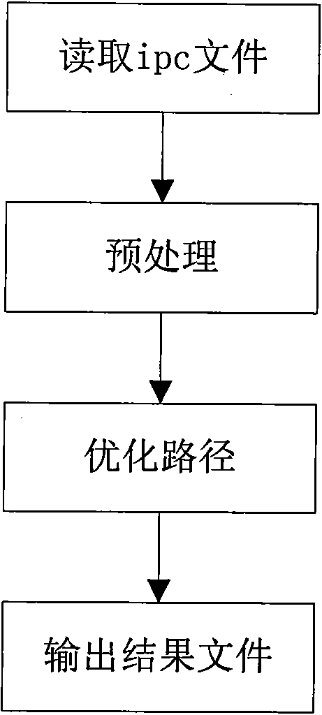
[0063] see figure 1 , a printed circuit board test path optimization method, the method comprises the steps of:

[0064] The method comprises the steps of:

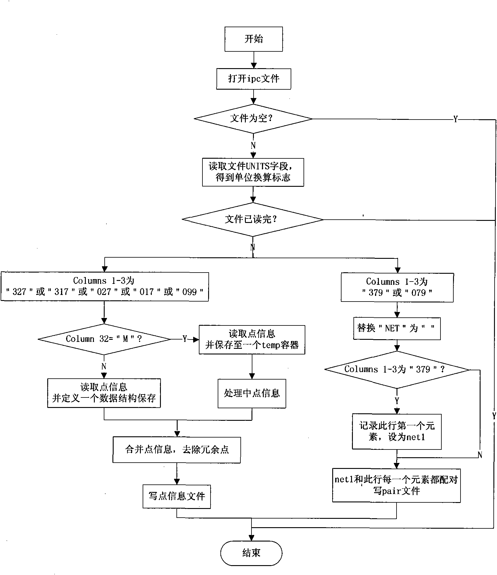
[0065] A. Read the ipc file to obtain the network number, front and back signs, coordinate information, and information of the adjacent network to which the point to be measured belongs;

[0066] The ipc file used in this method is a standard file in the flying probe testing industry, and its standard number is IPC-D-356: Test data format for the bare board of the bottom circuit board. Each line of the file will not exceed 80 characters. For each Character bits have strict definitions, which contain a lot of information, including point location information, size, board layers, etc., according to its strict bit definition, combined with the needs of short-circuit testing, we only need to read the file where the point to be tested belongs to The network number, front and back logo, coordinate information, and information...


PUM


Abstract

The invention discloses an optimization method of a printed-circuit board test path, which is characterized in that the optimization method comprises the following steps: A. reading an ipc file to obtain the network number, and the information of front and back mark and coordinate of a point to be tested, and information of adjacent networks; B. preprocessing the information; C. optimizing the path and E and outputting a test file: after open circuit is optimized, a CONTI.LST file is generated according to the standard of the IPC file. The information of all points and adjacent networks of thecircuit board to be tested are read by the ipc file, all network numbers are recombined and rearranged according to the principle of four-probe test, and the path of probe running is optimized as faras possible in the premise of not missing any networks, thus leading the path of probe running of a flying probe tester to be shortest; and by practical application, the result shows that the efficiency on testing time is improved by 3 percent to 16 percent compared with the existing software, therefore, the optimization method can be widely used in the manufacturing industry of printed-circuit boards and the electronic industry.

Description

technical field [0001] The invention relates to the technical field of printed circuit board testing, in particular to a method for optimizing a printed circuit board testing path. Background technique [0002] Printed circuit board (PCB) finished product inspection is an important link in the production process. The finished product inspection mainly checks whether the finished PCB has any failures such as open circuit, short circuit or line erosion. With the development of semiconductor technology, PCB has become more scaled and miniaturized, and its testing difficulty has also increased while its functions have been improved. According to statistics, the average cost of visual inspection in the field of electronic manufacturing can reach more than 50% of the cost of the entire manufacturing process. [0003] At this stage, the most commonly used testing methods for PCB are divided into non-vector testing technology and automatic imaging detection system, and the flying p...

Claims


Application Information

Patent Timeline
IPC IPC(8): G06F17/50
Inventor 周尚波胡鹏何革柳玉炯
Owner CHONGQING UNIV
Why Eureka
Try Eureka