Sensing module

A sensor and sensing area technology, which is applied to semiconductor devices, electrical components, circuits, etc., can solve the problems of inconvenience, high cost of packaging colloid 150, increased production cost of image sensing module 100, etc. The effect of improving light utilization efficiency

Active Publication Date: 2010-03-10
MICROSOFT TECH LICENSING LLC
View PDF0 Cites 7 Cited by
  • Summary
  • Abstract
  • Description
  • Claims
  • Application Information

AI Technical Summary

Problems solved by technology

[0004] However, since the cost of the encapsulant 150 is relatively high, the production cost of the image sensing module 100 will be increased.
In addition, the encapsulant 150 will reduce the intensity of the light provided by the laser diode 130, which will deteriorate the light utilization efficiency of the image sensing module 100.
[0005] It can be seen that the above-mentioned existing image sensing module obvio...

Method used


Image

  • Sensing module
  • Sensing module
  • Sensing module

Examples


Embodiment Construction

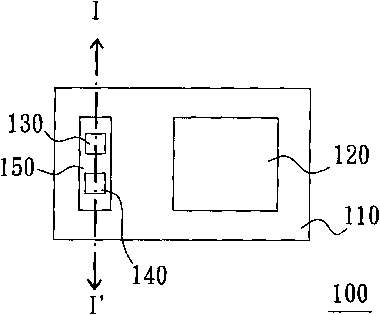
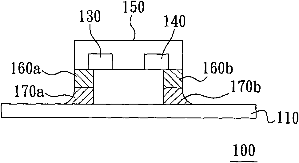
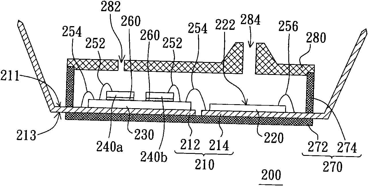
[0046] In order to further explain the technical means and effects of the present invention to achieve the intended purpose of the invention, the specific implementation, structure, features and effects of the sensing module proposed in accordance with the present invention will be described below with reference to the accompanying drawings and preferred embodiments. The detailed description is as follows.

[0047] The foregoing and other technical contents, features and effects of the present invention will be clearly presented in the following detailed description of the preferred embodiment with reference to the drawings. Through the description of the specific embodiments, it is possible to gain a more in-depth and specific understanding of the technical means and effects adopted by the present invention to achieve the predetermined purpose. However, the accompanying drawings are only for reference and explanation purposes, and are not used for the present invention. Be restr...


PUM


Abstract

The invention relates to a sensing module, which comprises a carrying device, a sensor, a substrate and a plurality of wafers, wherein the carrying device is provided with a carrying surface and a back surface opposite to the carrying surface; the sensor is arranged on the carrying surface and is electrically connected to the carrying device; the substrate is arranged on the carrying device and iselectrically connected to the carrying surface; and the plurality of wafers are arranged on the substrate and are electrically connected to the substrate respectively. In the sensing module, becausethe wafers are arranged on the substrate, the wafers and the substrate are not needed to be modularized by a transparent encapsulating colloid so as to reduce the production cost of the sensing module. In the embodiment that one of the wafers is a luminescent wafer, because the wafer is not needed to be covered by the transparent encapsulating colloid, the intensity of light rays provided by the luminescent wafer is not weakened by the transparent encapsulating colloid, and thus, the light utilization efficiency of the sensing module can be improved.

Description

Technical field [0001] The invention relates to a sensing module, in particular to a sensing module with multiple chips. Background technique [0002] figure 1 Is a top view of a conventional image sensing module, and figure 2 Is along figure 1 Sectional view of the I-I’ section line. Please refer to figure 1 versus figure 2 As shown, the conventional image sensor module 100 includes a printed circuit board (PCB) 110, an image sensor (image sensor) 120, a laser diode (LD) 130, and a Zener diode (Zenerdiode) 140 and an encapsulation 150. The image sensor 120 is disposed on the printed circuit board 110 and is electrically connected to the printed circuit board 110. The laser diode 130 and the Zener diode 140 are electrically connected to connection terminals 160a and 160b, respectively, and the connection terminals 160a and 160b are electrically connected to the printed circuit board 110 through tin materials 170a and 170b, respectively. [0003] In the prior art, the laser dio...

Claims


Application Information

Patent Timeline
IPC IPC(8): H01L25/16
CPCH01L2224/48091H01L2224/73265
Inventor 赖鸿庆李国雄陈晖暄王维中
Owner MICROSOFT TECH LICENSING LLC
Why Eureka
Try Eureka