
Partial block erase architecture for flash memory

A flash memory, memory block technology, applied in static memory, read-only memory, digital memory information and other directions, can solve problems such as complexity

Inactive Publication Date: 2010-03-24
CONVERSANT INTPROP MANAGEMENT INC
View PDF1 Cites 37 Cited by
  • Summary
  • Abstract
  • Description
  • Claims
  • Application Information

AI Technical Summary

Problems solved by technology

[0010] [0010] The problem is compounded by the fact that the block size of flash memory devices continues to increase while the size of the stored data files remains relatively constant

Method used


Image

  • Partial block erase architecture for flash memory
  • Partial block erase architecture for flash memory
  • Partial block erase architecture for flash memory

Examples


Embodiment Construction

[0035] [0020] In general, embodiments provide methods and systems for increasing the lifetime of flash memory devices. Each physical memory block of a flash memory device can be divided into at least two logical sub-blocks, where each of the at least two logical sub-blocks is erasable. Therefore, only the data of that logical block is erased and reprogrammed, while the unmodified data in other logical blocks avoids unnecessary program / erase cycles. The logical sub-blocks to be erased are dynamically configurable in terms of size and position within the block. Wear leveling algorithms are used to spread data across the physical and logical sub-blocks of the memory array to maximize the life of the physical blocks.

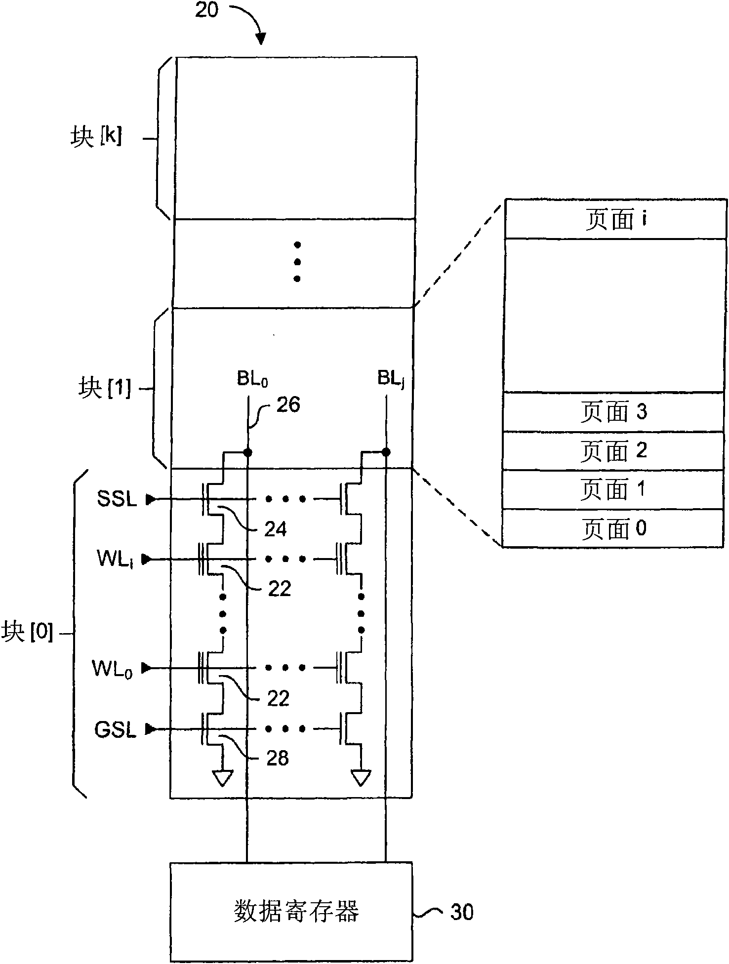
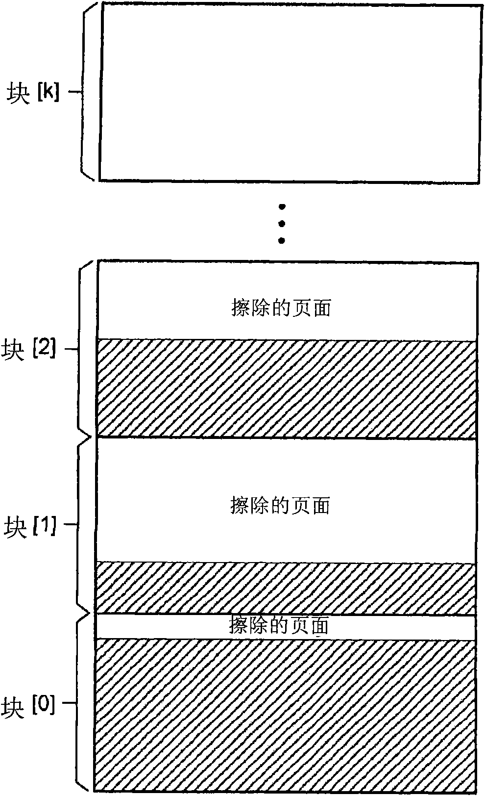
[0036] 【0021】 image 3 is a conceptual illustration of physical memory blocks (block[0] to block[k]) of the flash memory device according to the present embodiment. Each physical block can selectively erase logical sub-blocks, where the erased sub-blocks can incl...


PUM


Abstract

The invention provides a method and system for increasing the lifespan of a flash memory device by selectively erasing sub-blocks of a memory block. Each physical memory block of the flash memory device is dividable into at least two logical sub-blocks, where each of the at least two logical sub-blocks is erasable. Therefore, only the data of the logical sub-block is erased and reprogrammed whileunmodified data in the other logical sub-block avoids unnecessary program / erase cycles. The logical sub-blocks to be erased are dynamically configurable in size and location within the block. A wear leveling algorithm is used for distributing data throughout the physical and logical sub-blocks of the memory array to maximize the lifespan of the physical blocks during programming and data modification operations.

Description

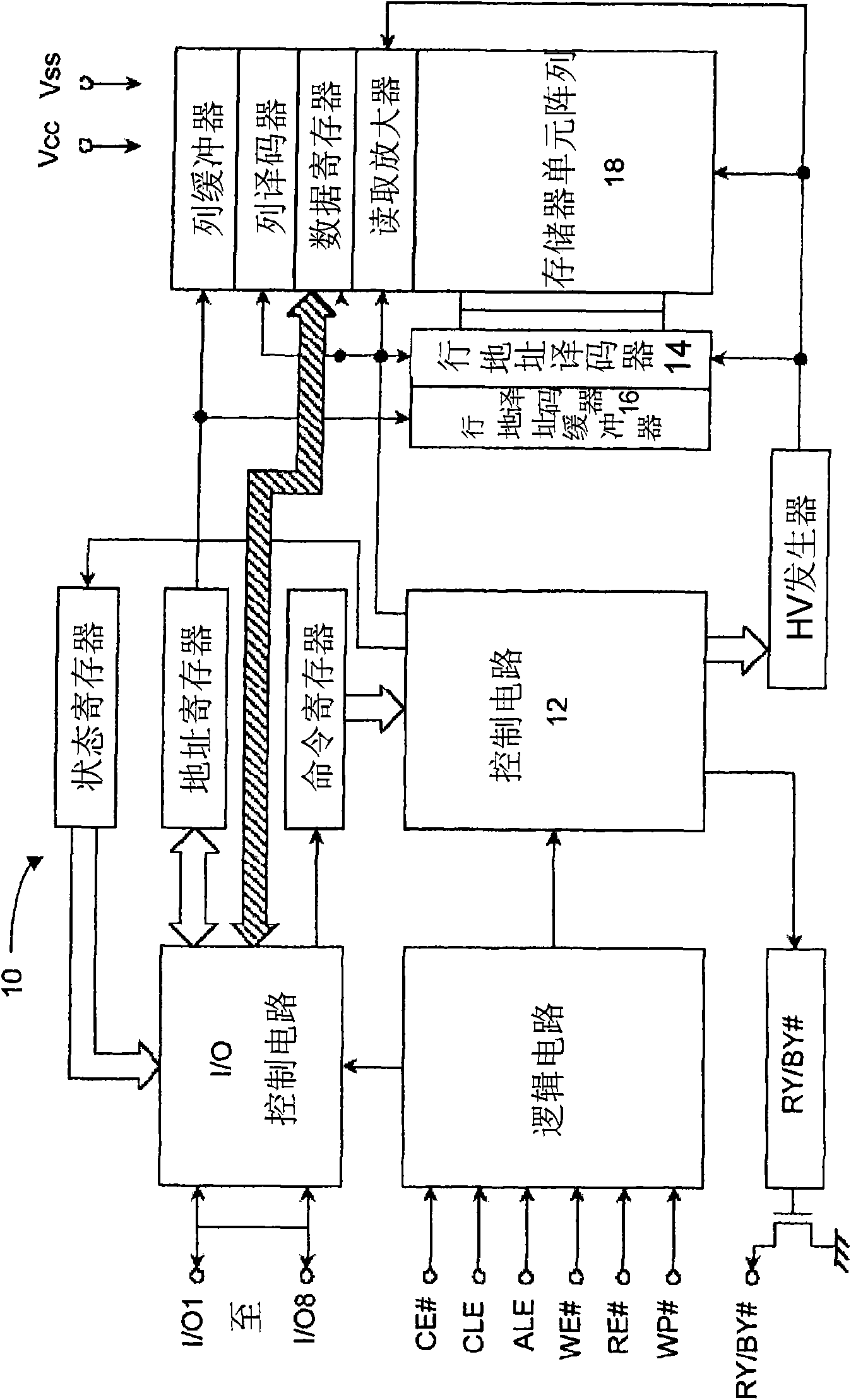
Background technique [0001] [0001] Flash memory is a common type of non-volatile memory widely used as a mass storage device in consumer electronic devices such as digital cameras and portable digital music players. The density of currently available flash memory chips can reach 32Gbit (4GB), which is suitable for use in popular USB flash drives due to the small size of a flash chip. [0002] [0002] FIG. 1 is a general block diagram of a typical flash memory of the prior art. The flash memory 10 includes a logic circuit such as a control circuit 12 for controlling a flash circuit of various functions, registers for holding address information, data information and command data information, and generating required programming and erasing voltages and core memory circuits such as row address decoder 14 and row address decoder buffer 16 for accessing memory array 18. Control circuitry 12 includes command decoders and logic for performing internal flash memory operations such as...

Claims


Application Information

Patent Timeline
Patent Type & Authority Applications(China)
IPC IPC(8): G11C16/16G11C16/02G11C16/08G11C7/20G11C8/14
CPCG11C16/344G11C16/349G11C16/3418G11C16/0483G11C16/3427G11C16/02G11C16/08G11C16/14G11C16/16
Inventor 金镇祺
Owner CONVERSANT INTPROP MANAGEMENT INC
Learn More