Organic el display panel

A technology of electroluminescence and display screen, applied in the field of organic EL display screen, can solve the problems of shortening the life of organic EL display screen, deterioration of organic light-emitting layer, reduction of luminous efficiency, etc., and achieves the effect of high aperture ratio, less deterioration and long life.

Active Publication Date: 2010-03-24
JOLED INC
View PDF17 Cites 39 Cited by
  • Summary
  • Abstract
  • Description
  • Claims
  • Application Information

AI Technical Summary

Problems solved by technology

Therefore, when the film thickness of the organic light-emitting layer in the sub-pixel is not uniform, the aperture ratio decreases and the luminous efficiency decreases.
[0034]Furthermore, when only the organic light-emitting layer in the center part emits light, the organic light-emitting layer in the center part deteriorates remarkably, which becomes one cause of shortening the life of the organic EL display panel

Method used


Image

  • Organic el display panel
  • Organic el display panel
  • Organic el display panel

Examples


Embodiment approach 1

[0146] In Embodiment 1, an active matrix type organic EL display panel will be described.

[0147] Figure 4 It is a plan view of the organic EL display panel 100 of the first embodiment. Such as Figure 4 As shown, the organic EL display panel 100 has: a cathode 111 covering the entire panel.

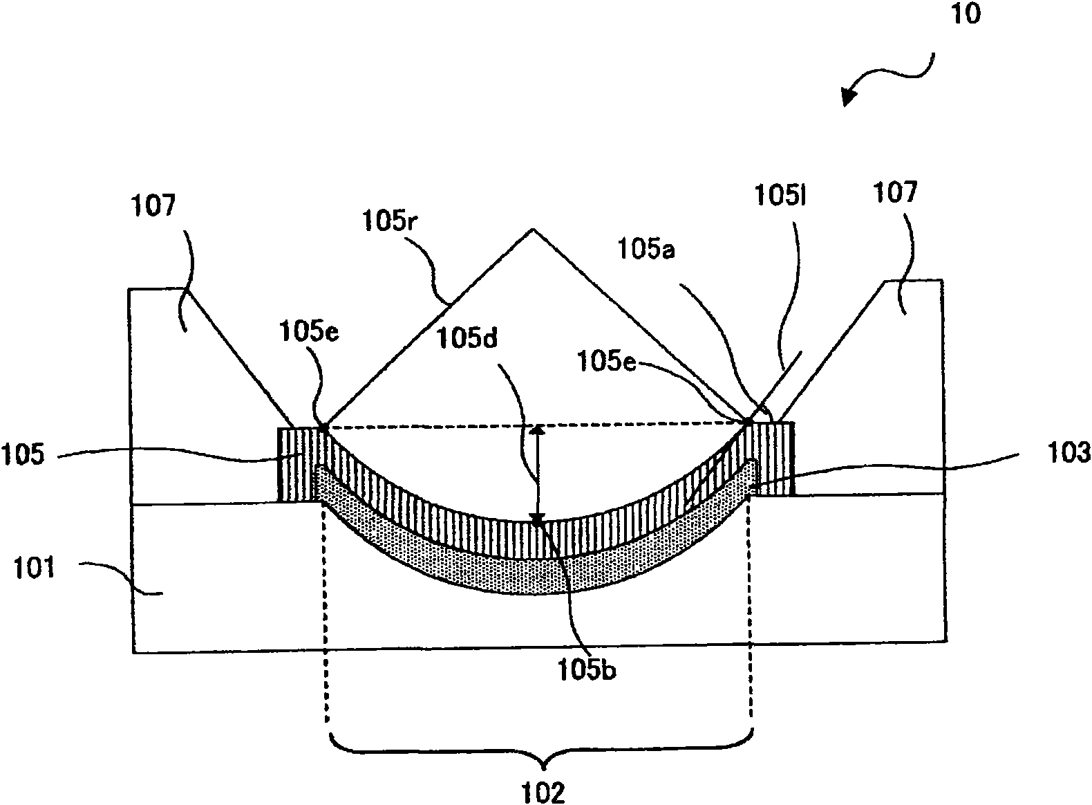
[0148] Figure 5 It is a plan view of the organic EL panel 100 omitting the cathode 111 . Such as Figure 5 As shown, the organic EL display panel 100 has linear banks 107 arranged on a substrate 101 in parallel with each other. The linear banks 107 define the linear region 11 . In the linear region 11, a plurality of organic EL elements 10 are arranged in a row. Furthermore, a linear organic light emitting layer 109 is arranged in the linear region 11 . The organic EL elements 10 arranged in the linear region 11 share the linear organic light emitting layer 109 .

[0149] The organic EL elements 10 arranged in the linear region 11R emit red light, the organic EL elements 10 a...

Embodiment approach 2

[0158] In Embodiment 1, an example in which the surface of the concavely curved hole transport layer is parabolic cylindrical is described. In Embodiment 2, an example in which the surface of the concavely curved hole transport layer is an elliptical paraboloid will be described.

[0159] Figure 8 It is a perspective view of the organic EL display panel 200 of Embodiment 2 omitting a cathode, an organic light-emitting layer, and an intermediate layer. The organic EL display panel 200 is the same as the organic EL display panel 100 except that the substrate 101 has the shape of the concave portion 102a. Therefore, the same reference numerals are attached to the same constituent elements as those of the organic EL display panel 100, and description thereof will be omitted.

[0160] Such as Figure 8 As shown, the substrate 101 has concave and curved portions 102 a arranged in a row in the linear region 11 . The concave portion 102a has an elliptical paraboloid-shaped surfac...

Embodiment approach 3

[0163] In Embodiment 1 and Embodiment 2, the structure of the banks is described as an example of a one-layer structure. In Embodiment 3, an example in which the bank structure is a two-story structure will be described.

[0164] The plan view of the organic EL display panel of Embodiment 3 and the Figure 4 and Figure 5 The plan view of the organic EL display panel 100 of Embodiment 1 shown is the same.

[0165] Figure 9 It is a sectional view of the organic EL element 20 included in the organic EL display panel of the third embodiment. The organic EL element 20 is the same as the organic EL element 10 except that it has an inorganic film. Therefore, the same reference numerals are assigned to the same constituent elements as those of the organic EL element 10, and description thereof will be omitted.

[0166] Such as Figure 9 As shown, the organic EL element 20 has the inorganic film 106 in the lower layer of the bank 107 . The inorganic film 106 is arranged on the...


PUM


Abstract

Disclosed is an organic EL display panel with an organic light emitting layer of a uniform film thickness. The organic EL display panel comprises a substrate, a line-shaped bank that is arranged on the substrate and defines line-shaped regions on the substrate, and two or more organic EL elements arranged in a row in each of the line-shaped regions. Each of the organic EL elements includes an anode arranged on the substrate, a hole injection layer arranged on the anode and comprised of a metal oxide, an organic light emitting layer arranged on the hole injection layer, and a cathode arranged on the organic light emitting layer. The hole injection layer is formed in a concave or convex shape, a part of the hole injection layer is arranged below the bank, and the organic light emitting layeris formed by coating the line-shaped regions with an organic light emitting material.

Description

technical field [0001] The present invention relates to an organic EL (Electroluminescent: electroluminescence) display screen and a manufacturing method of the organic EL display screen. Background technique [0002] An organic EL device as a display device is a light-emitting element utilizing electroluminescence of an organic compound. The organic EL device includes: a cathode and an anode, and an organic light-emitting layer arranged between the two electrodes for electroluminescence. Organic compounds contained in an organic light-emitting layer that performs electroluminescence can be roughly classified into combinations of low-molecular organic compounds (host material and dopant material) and high-molecular organic compounds. Examples of high-molecular organic compounds that perform electroluminescence include polyphenylenevinylene called PPV or derivatives thereof. Organic EL devices using high-molecular organic compounds can be driven at a relatively low voltage,...

Claims


Application Information

Patent Timeline
Patent Type & Authority Applications(China)
IPC IPC(8): H01L51/50H05B33/10H05B33/12H05B33/26
CPCH01L51/5262H01L51/5088H01L51/5206A23V2250/5114H01L27/3246H01L51/0003A23V2200/22H01L27/3283H10K59/124H10K59/173H10K59/122H10K71/12H10K50/17H10K50/813H10K50/85H10K2102/301
Inventor 吉田英博奥本健二山室景成
Owner JOLED INC
Why Eureka
Try Eureka