Method for the production of laminated ceramic electronic parts

A technology of electronic components and manufacturing methods, which is applied in the field of manufacturing laminated ceramic electronic components, can solve the problems of shrinking force of the constraining layer, obstacles, difficulty in removing the constraining layer, etc., and achieve improved binding force and high-precision manufacturing Effect

Inactive Publication Date: 2010-03-24
MURATA MFG CO LTD
View PDF1 Cites 2 Cited by
  • Summary
  • Abstract
  • Description
  • Claims
  • Application Information

AI Technical Summary

Problems solved by technology

However, conversely, it will cause problems that it is difficult to remove the constraining layer and the reaction product
[0014] On the other hand, if the particle size of the inorganic powder in the constrained layer is increased, the glass in the substrate layer and the inorganic powder particles in the constrained layer are difficult to react, so it is easy to remove the constrained layer, but the constrained layer can suppress shrinkage in the plane direction. The force becomes smaller, in which case it is sometimes impossible to restrain its contraction
[0015] Therefore, it is of great significance to adjust the particle size of the inorganic powder in the constrained layer, but it is very difficult to obtain the high confinement of the constrained layer and the easy removal of the constrained layer at the same time, which becomes an obstacle in the implementation of the non-shrinkage process

Method used


Image

  • Method for the production of laminated ceramic electronic parts
  • Method for the production of laminated ceramic electronic parts
  • Method for the production of laminated ceramic electronic parts

Examples


Embodiment Construction

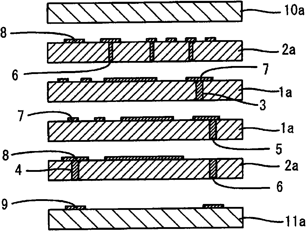
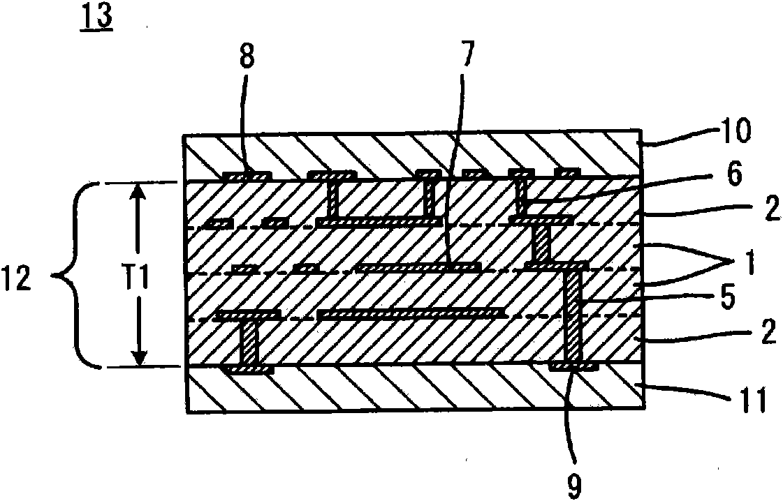
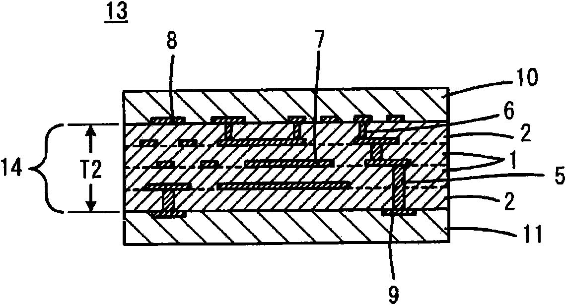
[0050] Figure 1 to Figure 4 It is a sectional view for demonstrating the manufacturing method of the multilayer ceramic electronic component which concerns on one Embodiment of this invention. In particular, a method of manufacturing a multilayer ceramic substrate is shown here.

[0051] First, if figure 1 As shown, prepare the first substrate layer 1 to be green (refer to figure 2 ) green body 1a for the first base material layer, and prepare the second base material layer 2 to be unsintered (refer to figure 2 ) The green body 2a for the second substrate layer. The green body 1a for the 1st base material layer and the green body 2a for the 2nd base material layer contain the 1st and 2nd low temperature sinterable ceramic powder, respectively. These substrate layer green bodies 1a and 2a are produced by dispersing the above-mentioned low-temperature sinterable ceramic powder in a vehicle formed of a binder, a solvent, a plasticizer, etc. to prepare a slurry, and then us...


PUM

PropertyMeasurementUnit
particle sizeaaaaaaaaaa

Abstract

A method of producing a multi-layer ceramic substrate by firing in a state where bonding layers which are not sintered during firing are arranged on the principal surfaces of an unsintered ceramic laminate and then the bonding layers are removed, wherein removal of the bonding layers becomes more difficult if the bonding strength of the bonding layers is high, whereas the bonding layers can be removed easily if the bonding strength is low. A conductor pattern (5 - 9) which contains Ag as the main component is formed and first base material layers (1) and second base material layers (2) are laminated in the unsintered ceramic laminate (12). The second base material layers (2) are arranged along at least one principal surface of the unsintered ceramic laminate (12) and the bonding layers (10, 11) are arranged so as to be in contact with the second base material layers (2). A composition in which during firing Ag diffuses more easily into the second base material layers (2) than into thefirst base material layers (1) is employed and the bonding strength is improved by reducing the glass softening point without the need to use a means of reducing the particle size of the ceramic powder contained in the bonding layers, which is not readily sintered.

Description

technical field [0001] The present invention relates to a method of manufacturing laminated ceramic electronic components, and more particularly to a method of manufacturing laminated ceramic electronic components using a so-called shrink-free process. Background technique [0002] A multilayer ceramic substrate, which is an example of a multilayer ceramic electronic component, has a plurality of laminated ceramic layers, and usually a conductive pattern is formed on the surface or inside. The conductor pattern includes, for example, an in-plane conductor extending in the planar direction of the ceramic layer, and an interlayer connection conductor (typically a via-hole conductor) extending so as to penetrate the ceramic layer in the thickness direction. [0003] In general, such a multilayer ceramic substrate mounts surface-mount electronic components such as semiconductor devices and chip stack capacitors thereon, and interconnects these surface-mount electronic components...

Claims


Application Information

Patent Timeline
Patent Type & Authority Applications(China)
IPC IPC(8): H05K3/46H01G4/12H01G4/30
CPCH05K3/4688H05K3/4629H01G4/12H05K1/0306H05K2203/308H05K3/4614H01G4/232H01G4/30H01L2924/19105H01L2224/16225H01L2924/15192H05K3/46
Inventor 近川修池田哲也
Owner MURATA MFG CO LTD
Why Eureka
Try Eureka