PIN Si-based film solar battery and manufacturing method thereof

A technology of solar cells and silicon-based thin films, which is applied in circuits, photovoltaic power generation, electrical components, etc., can solve the problems of industrialization of solar cells, and achieve the effects of reducing interface defects, increasing carrier mobility, and improving efficiency

Inactive Publication Date: 2010-04-28
NANJING UNIV OF AERONAUTICS & ASTRONAUTICS
View PDF0 Cites 16 Cited by
  • Summary
  • Abstract
  • Description
  • Claims
  • Application Information

AI Technical Summary

Problems solved by technology

There is no industrialization of the formation of thin film

Method used


Image

  • PIN Si-based film solar battery and manufacturing method thereof
  • PIN Si-based film solar battery and manufacturing method thereof
  • PIN Si-based film solar battery and manufacturing method thereof

Examples


Embodiment 1

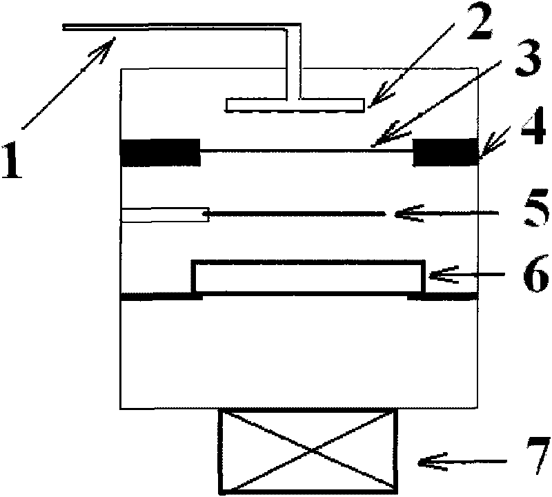
[0019] A silicon-based thin-film PIN junction solar cell, adopting hot filament chemical vapor deposition on a transparent conductive glass to successively deposit the P-layer, I-layer, dielectric passivation layer and the P-layer of the silicon-based thin-film solar cell core-PIN junction N-tier. Concrete preparation process is as follows:

[0020] 1. Put the cleaned transparent conductive film substrate into the chamber, raise the temperature, and evacuate the chamber to a suitable background vacuum value.

[0021] 2. When the substrate temperature and vacuum degree meet the requirements, grow the P-layer. The specific parameters are as follows:

[0022] Flow ratio: SiH 4 :B 2 h 6 =1:0.01, the dilution ratio is controlled at 91%, the air pressure is controlled at 2Pa, the substrate temperature is 250°C, the temperature of the hot wire is controlled at ~1900°C, the distance between the substrate and the hot wire is controlled at 5cm, and the film thickness is controlled a...

Embodiment 2

[0032] A silicon-based thin-film PIN junction solar cell, adopting hot filament chemical vapor deposition on a transparent conductive glass to successively deposit the P-layer, I-layer, dielectric passivation layer and the P-layer of the silicon-based thin-film solar cell core-PIN junction N-tier. Concrete preparation process is as follows:

[0033] 1. Put the cleaned transparent conductive film substrate into the chamber, raise the temperature, and evacuate the chamber to a suitable background vacuum value.

[0034] 2. When the substrate temperature and vacuum degree meet the requirements, grow the P-layer. The specific parameters are as follows:

[0035] Flow ratio: SiH 4 :B 2 h 6=1:0.01, the dilution ratio is controlled at 91%, the air pressure is controlled at 2Pa, the substrate temperature is 250°C, the temperature of the hot wire is controlled at ~1900°C, the distance between the substrate and the hot wire is controlled at 5cm, and the film thickness is controlled at...

Embodiment 3

[0045] A silicon-based thin-film PIN junction solar cell, adopting hot filament chemical vapor deposition on a transparent conductive glass to successively deposit the P-layer, I-layer, dielectric passivation layer and the P-layer of the silicon-based thin-film solar cell core-PIN junction N-tier. Concrete preparation process is as follows:

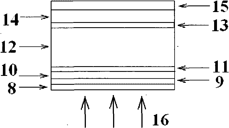
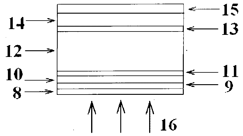
[0046] The preparation process of silicon-based thin-film PIN junction solar cells. The process steps are: use transparent conductive glass as the substrate, and grow the P-layer on it by hot wire chemical vapor deposition. The growth process is as follows: Flow ratio: SiH 4 :B 2 h 6 =1:0.01, the dilution ratio is controlled at 90%, the air pressure is controlled at 1Pa, the substrate temperature is 150°C, the temperature of the hot wire is controlled at 1800°C, the distance between the substrate and the hot wire is controlled at 3cm, and the film thickness is controlled at 10nm; A layer of silicon nitride dielectric material is grown ...


PUM

PropertyMeasurementUnit
Thicknessaaaaaaaaaa
Thicknessaaaaaaaaaa
Short circuit currentaaaaaaaaaa

Abstract

The invention belongs to the technical field of solar battery devices, and relates to a PIN junction Si-based film solar battery and a preparation process thereof. Concretely, a first P layer, a first I layer and a first N layer of a PIN junction of the core of the Si-based film solar battery are prepared by using a hot filament chemical vapor deposition method by which a passivation layer made of dielectric materials grows between the first P layer and the first I layer. The hot filament chemical vapor deposition method has the advantages of high air source usage, rapid growth speed, reduced interface defect and the like. Compared with the film grown by a PECVD method, the film in the invention has higher H content and less dangling bonds and better film quality. In addition, the passivation layer between the first P layer and the first I layer can passivate the dangling bonds on the interface and increase current carrier mobility at the interface position by tunnel effect, thus greatly improving battery efficiency.

Description

technical field [0001] The invention belongs to the technical field of solar cell devices, and relates to a PIN junction silicon-based thin-film solar cell and a preparation process thereof. Specifically, the P-layer, I-layer, and N-layer of the core-PIN junction of silicon thin film solar cells are prepared by hot-filament chemical vapor deposition, and the P-layer A passivation layer composed of a dielectric material is grown between the I-layer and the I-layer. Background technique [0002] Solar energy is one of the most important renewable and clean energy available to human beings. Solar power generation is another very important application in the use of solar energy. At present, solar cells mainly include crystalline silicon solar cells and silicon thin film solar cells. Silicon is one of the most abundant elements on earth, and it is environmentally friendly and non-toxic. Compared with crystalline silicon solar cells, silicon thin-film solar cells have more adv...

Claims


Application Information

Patent Timeline
IPC IPC(8): H01L31/042H01L31/18H01L31/0445H01L31/075
CPCY02E10/50Y02E10/548Y02P70/50
Inventor 沈鸿烈黄海宾吴天如鲁林峰
Owner NANJING UNIV OF AERONAUTICS & ASTRONAUTICS
Why Eureka
Try Eureka