Manufacture method of golden finger printed board

A manufacturing method and gold finger technology, which is applied in the reinforcement of conductive patterns, the secondary treatment of printed circuits, the formation of electrical connections of printed components, etc., can solve the problems of low efficiency, complicated process flow, and increased material costs, and reduce the cost of leads. Design, convenience of gold plating layer, and the effect of improving production efficiency

Active Publication Date: 2010-04-28
GUANGZHOU FASTPRINT CIRCUIT TECH
View PDF0 Cites 55 Cited by
  • Summary
  • Abstract
  • Description
  • Claims
  • Application Information

AI Technical Summary

Problems solved by technology

This method can make long and short gold fingers, but it increases the cost of materials, and the process is complicated and the efficiency is low

Method used


Image

  • Manufacture method of golden finger printed board
  • Manufacture method of golden finger printed board
  • Manufacture method of golden finger printed board

Examples


Embodiment

[0023] A kind of manufacturing method of golden finger printed board, it comprises the following steps:

[0024] a. Inner layer graphic production, the inner layer board can be made according to the design requirements;

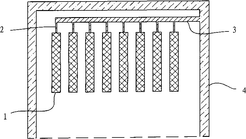
[0025] b. Lamination, drilling, copper sinking, board surface electroplating;

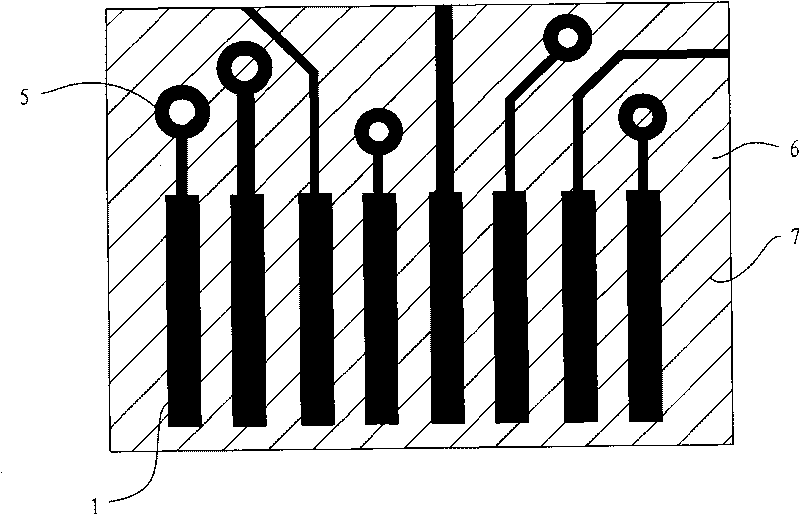
[0026] c. The first outer graphics transfer: refer to figure 2 , make the outer layer circuit graphics on the outer layer board, the graphic of the film used is the outer layer circuit graphic, and the graphic part is black, light blocking, the non-graphic part is transparent, light transmission, at a pressure of 0.2-0.6Mpa, a temperature of 90- Under the condition of 130°C, the first layer of dry film (photoresist film) is pasted on both sides of the printed board. After exposure to 5-12 levels of ultraviolet energy, it is developed with a weak alkali solution of sodium carbonate. It can be developed according to the circuit According to the type of board and the type of dry f...


PUM

PropertyMeasurementUnit
thicknessaaaaaaaaaa
thicknessaaaaaaaaaa
thicknessaaaaaaaaaa

Abstract

The invention discloses a manufacture method of a golden finger printed board, which comprises the steps of: producing a normal inner pattern, laminating, drilling, depositing copper, electroplating a board surface, and firstly transferring an outer layer pattern, wherein the copper surface of a pattern part of a circuit on an outer layer board is exposed, and a non-pattern part is covered by a first layer dry film; electroplating copper nickel golden on a circuit board, so that the pattern part which is not covered with the first layer dry film is plated with the copper by means of thickening, and a nickel layer and a normal golden layer is plated thereon; secondly transferring the outer layer pattern, arranging a light-resistant through window at the golden finger part of the film pattern, exposing the other part, and covering a second layer dry film on the board surface; exposing and developing, exposing a normal golden layer of the golden finger part in the window, and respectively covering the first layer dry film or the second layer dry film or the two layer dry films at the other part; and plating a hard golden layer, removing the film, and etching the outer layer. The manufacture method reduces a step for removing a golden finger lead wire, has a flexible designing way, saves cost, and improves production efficiency.

Description

technical field [0001] The invention relates to a method for manufacturing a printed circuit board, in particular to a method for manufacturing a printed circuit board with golden fingers. Background technique [0002] With the continuous development of electronic products in the direction of multi-functionality, miniaturization, light weight and high performance, the requirements for miniaturization and high density of printed circuit boards are also increasing, and its products are also changing from traditional printed circuit boards to high-density Build-up printed board development. The key to the production of high-density laminated printed boards is the realization of ultra-high density and high reliability. Gold has good electrical conductivity, chemical stability and solderability. The gold plating layer is flat, bright, and has high corrosion resistance. It meets the high reliability requirements of high-density laminated printed boards, so its application range i...

Claims


Application Information

Patent Timeline
Patent Type & Authority Applications(China)
IPC IPC(8): H05K3/40H05K3/24
Inventor 李志东乔书晓张锐
Owner GUANGZHOU FASTPRINT CIRCUIT TECH
Why Eureka
Try Eureka