Base region structure of triode
A transistor and base technology, applied in transistors, electrical components, circuits, etc., can solve problems such as germanium-silicon lattice mismatch, and achieve the effect of improving performance, reducing base resistance, and not easy to lattice adaptation.
- Summary
- Abstract
- Description
- Claims
- Application Information
AI Technical Summary
Problems solved by technology
Method used
Image

Examples
Embodiment Construction
[0016] Below, the present invention will be further described in conjunction with the accompanying drawings.
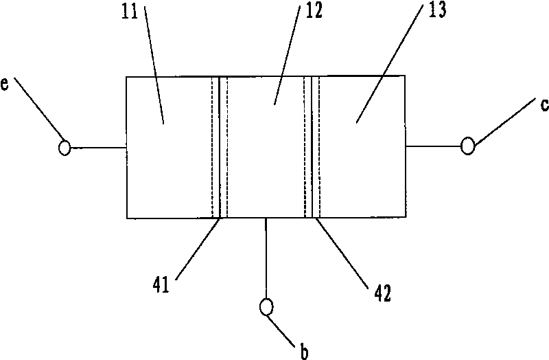
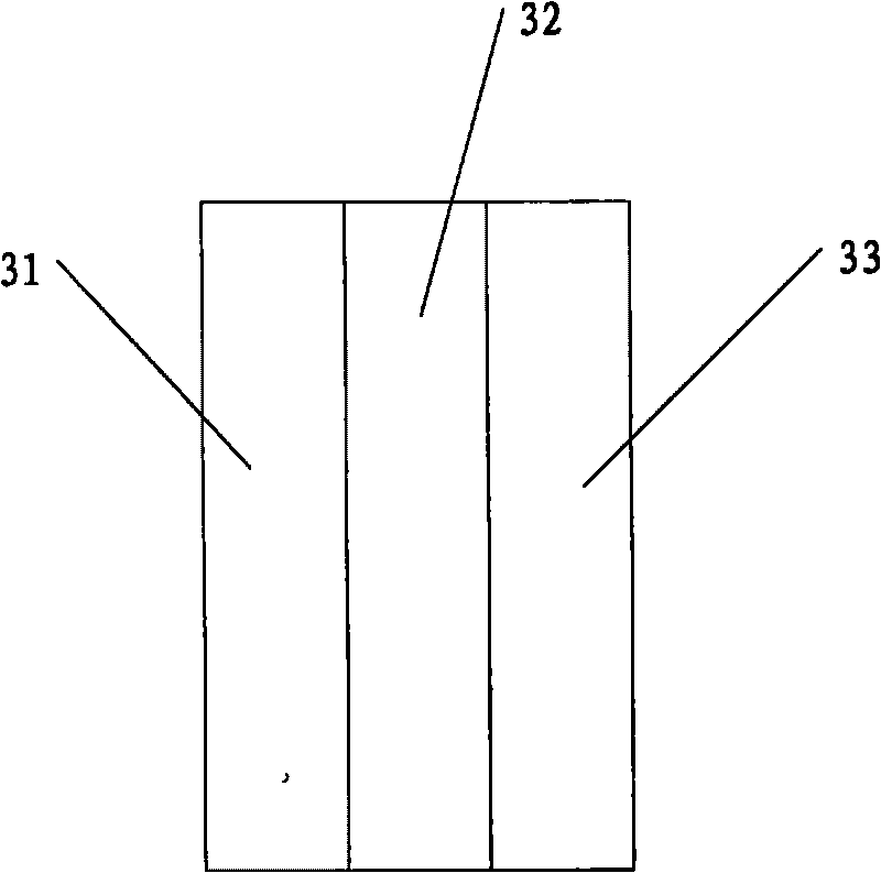
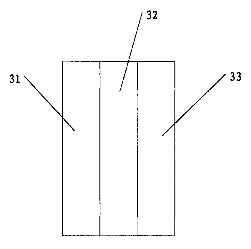
[0017] The present invention proposes a triode base region structure, the triode includes an emitter region, a base region and a collector region, and the base region is located between the emitter region and the collector region. Below, please refer to figure 2 , figure 2 It is a schematic diagram of the base structure of a triode according to the present invention. It can be seen from the figure that the base includes an undoped polysilicon layer 31, a silicon germanium layer or a germanium layer formed sequentially from the side of the collector region to the side of the emitter region. A silicon carbon layer 32 and a doped polysilicon layer 33, wherein the non-doped polysilicon layer 31 is connected to the collector region, and the doped polysilicon layer 33 is connected to the emitter region. The thickness range of the undoped polysilicon layer is 0.1 nanomet...
PUM
| Property | Measurement | Unit |
|---|---|---|
| Thickness | aaaaa | aaaaa |
Abstract
Description
Claims
Application Information
 - R&D
- Intellectual Property
- Life Sciences
- Materials
- Tech Scout
- Unparalleled Data Quality
- Higher Quality Content
- 60% Fewer Hallucinations
Browse by: Latest US Patents, China's latest patents, Technical Efficacy Thesaurus, Application Domain, Technology Topic, Popular Technical Reports.
© 2025 PatSnap. All rights reserved.Legal|Privacy policy|Modern Slavery Act Transparency Statement|Sitemap|About US| Contact US: help@patsnap.com