

Novel plasma display panel
A display panel and plasma technology, applied in alternating current plasma display panels, tube structural parts, maintenance/scanning electrodes, etc., can solve the problem of display brightness blocking, and achieve the effect of improving scanning speed, high light efficiency, and low ignition voltage
- Summary
- Abstract
- Description
- Claims
- Application Information
AI Technical Summary
Problems solved by technology
Method used
Image

Examples
Embodiment Construction
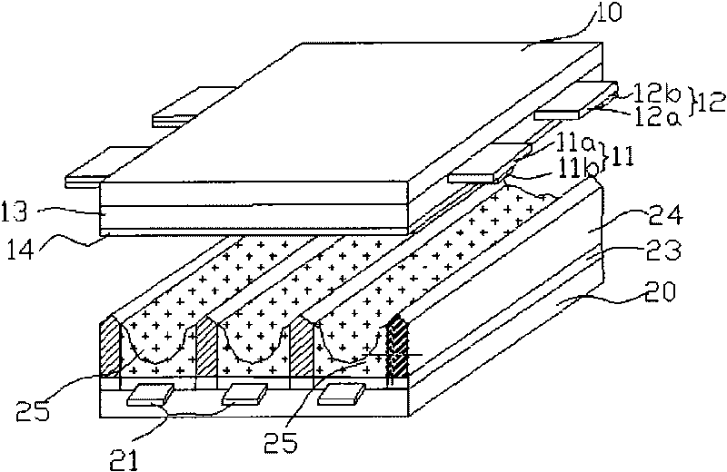
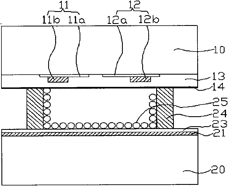
[0031] Refer below Figure 5 to Figure 8 , the structure and design of the plasma display screen according to the present invention will be described in detail.
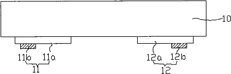
[0032] Figure 5 The electrode structure layout diagram of the front substrate according to the present invention. Such as Figure 5 As shown, the scan electrode 11 is composed of a metal electrode 11b with a light leakage hole 11k, and the sustain electrode 12 is composed of a transparent electrode 12a and a silver electrode (bus electrode) 12b on the transparent electrode 12a. Wherein, the discharge portion of the scan electrode is an arc-shaped bulge formed from the entire metal electrode. The silver electrode 12b can reduce the voltage drop of the transparent electrode 12a during PDP operation, and improve the scanning efficiency.
[0033] Figure 6a , Figure 6b and Figure 6c It is a plan view of the electrode arrangement of the front substrate in the present invention. Such as Figure 6a As shown, the...
PUM
 Abstract
Description
Claims
Application Information