Method for manufacturing silicon substrate GaN-based semiconductor material

A manufacturing method and technology of silicon substrates, applied in semiconductor/solid-state device manufacturing, electrical components, circuits, etc., can solve the problems of unstable growth and low production efficiency

Inactive Publication Date: 2010-06-02
LATTICE POWER CHANGZHOU
View PDF3 Cites 10 Cited by
  • Summary
  • Abstract
  • Description
  • Claims
  • Application Information

AI Technical Summary

Problems solved by technology

[0019] The problem to be solved by the present invention is to provide a method for manufacturing a GaN-based semiconductor

Method used


Image

  • Method for manufacturing silicon substrate GaN-based semiconductor material
  • Method for manufacturing silicon substrate GaN-based semiconductor material
  • Method for manufacturing silicon substrate GaN-based semiconductor material

Examples


Embodiment 1

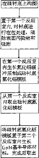
[0044] Based on the above conditions, for a silicon substrate sheet that has been patterned and grooved, the first embodiment of the method for producing a GaN-based semiconductor material on a silicon substrate according to the present invention is as follows:

[0045] 1. Silicon substrate in-situ high-temperature hydrogen treatment: put the silicon substrate into the first reaction chamber, and perform in-situ treatment on the silicon substrate under a relatively high temperature and hydrogen-containing atmosphere to remove the impurities on the substrate. organic pollutants and adsorbed oxygen atoms.

[0046] 2. After the in-situ processing of the silicon substrate is completed, the temperature is lowered to prepare for the growth of aluminum nitride. The growth temperature of aluminum nitride is 500-1000 degrees Celsius.

[0047] 3. In order to realize the transition from Si lattice to AlN lattice smoothly, a trimethylaluminum source can be introduced into the first reacti...

Embodiment 2

[0052] Compared with Example 1, the difference is that the above steps 3 and 4 are changed to: first inject ammonia gas to form a thin layer of SiN, and then grow AlN with a thickness of 1200 angstroms.

Embodiment 3

[0054] The difference compared with the first embodiment is that the above steps three and four are changed: in the process of forming the aluminum nitride buffer layer on the silicon substrate, the high-pressure growth is performed first, and then the low-pressure growth is performed.


PUM

PropertyMeasurementUnit
Thicknessaaaaaaaaaa
Thicknessaaaaaaaaaa

Abstract

The invention provides a method for manufacturing a silicon substrate GaN-based semiconductor material, aiming at solving the problem of re-melting a silicon surface by Ga in the process of extending GaN-based semiconductor material to improve the quality of the product and the production efficiency. The method comprises the following steps of: generating an aluminum nitride buffer layer on the silicon substrate in a reaction chamber of a first MOCVD specially for growing the aluminum nitride buffer layer, and taking out the aluminum nitride buffer layer after the step is completed to form a silicon substrate aluminum nitride template for later use; and placing the silicon substrate aluminum nitride template for later use into a reactor of a second MOCVD for growing a GaN-based semiconductor material to extend the GaN-based semiconductor material; and taking out the silicon substrate aluminum nitride template after the step is completed to form a silicon substrate GaN-based semiconductor material. The method can be applied to production manufacture of light-emitting diodes, diode lasers, power devices and the like.

Description

technical field [0001] The invention relates to a method for manufacturing a GaN-based semiconductor material, in particular to a method for manufacturing a GaN-based semiconductor material with silicon as a growth substrate. Background technique [0002] In the prior art, GaN-based semiconductor materials are produced on silicon substrates, and AlN and GaN epitaxial layers are sequentially grown on silicon substrates from bottom to top in MOCVD equipment. [0003] In the journal "Semiconductor Technology" in 2006, Volume 31, Issue 02, there is a paper "Research on GaN-based Materials and Devices on Si Substrates", which is listed in the Chinese Library Classification Number: TN316 Document Identification Code: A , article number: 1003-353X(2006)02-0098-04. [0004] This paper clearly records a current method for producing GaN-based semiconductor materials on silicon substrates. [0005] Since the epitaxial GaN on the Si substrate has a lattice mismatch of 17%, the lattice...

Claims


Application Information

Patent Timeline
IPC IPC(8): H01L21/205
Inventor 江风益方文卿郑畅达莫春兰王立
Owner LATTICE POWER CHANGZHOU
Why Eureka
Try Eureka